No idea what G0.001 means. Tried looking up all the FET parameters to see if anything looked applicable and the only thing maybe remotely related would be gate leakage current.
That is from the attached file (lot of useful info in there)
IGSS (gate leakage current) guarantees the maximum leakage current through the gate of the MOSFET. The IGSS is important when calculating how much current is required to keep the device turned on. Because it is a leakage current through an insulator, this current is independent of temperature, unlike IDSS.
That is from the attached file (lot of useful info in there)
Attachments
Some interesting developments on this MCP73831 model, after sharing with the ltspice group.
A few of my errors were corrected, but some alterations are bringing this a little closer to something that may work.
No more schottky diodes on the mosfets, but maybe they have no real influence.
Perhaps the little gig up there where the mystery box is may be interesting.
I ran some sims and found my idea of using a big cap as an R/C setup as a battery not so good, so I tried something else, with a voltage source with a delay to turn on followed by a ramp up to fake a charging battery. But then there is no real way of telling if the behavior is only due to that or if the IC decides things.
The screenshot does show one thing that seems consistent, the voltage source used to simulate the battery goes up to 3.6V, which would be the max voltage of a fully charged battery, but the Vbat does rise to about 4.1V.
This seems to be consistent with having the chip variant pre-configured for 4.1V max charge voltage, which is a factory set parameter.
This brings me to think that the datasheet's schematic is showing the resistor values for that variant configuration of the chip. I'm sure those values change depending on the factory configuration chosen for the variant.
I use a pulse with a delay before voltage is applied on Vdd, to simulate the arrival of power some time after the actual start of the simulation, so there is supposed to be no power for the chip, however we do have current sources there, and resistors, causing voltage drops from that flowing current, so the circuit does show voltages before anything is actually applied to Vdd.
Not so easy to simulate this thing.
Attachments
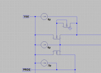
Here is how Linear Tech simulate a battery. Maybe LT have a similar chip to the one you are trying to simulate.
Solutions - LTM8062 Basic 2A, 4-Cell Li-Ion Battery Charger with C/10 Termination
Try the simulation file.
Solutions - LTM8062 Basic 2A, 4-Cell Li-Ion Battery Charger with C/10 Termination
Try the simulation file.
Here is how Linear Tech simulate a battery. Maybe LT have a similar chip to the one you are trying to simulate.
Solutions - LTM8062 Basic 2A, 4-Cell Li-Ion Battery Charger with C/10 Termination
Try the simulation file.
Wow! Yes, I'll try this right away.
Turns out I wasn't very far off about a simulated battery.
We're making good progress on that MCP73831 model.
Using the Linear method to fake out a battery and the "startup" option for the tran statement, I changed back the Vdd power supply source to a normal DC instead of pulse.
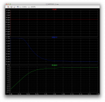
A few tweaks and got it to behave somewhat like a charging circuit, although it's not yet behaving quite like the specs dictate.
For one thing the stat output doesn't work, and the resistor on prog has no effect.
There is no trickle charge phase that I can see for a deeply deplete battery. I used 0.2V for the battery starting voltage, so I assume this should make it have a pre-conditioning trickle phase before entering the constant current one, but it's not exhibiting that behavior.
However it does show a 1st phase for the constant current, although not at the current value that is supposed to be determined by the res value on prog. That res on prog has no effect.
The value of 67k should bring the constant charging current at 14.5mA per spec, and 10k should bring it to 100mA. Instead it's staying at 2.7mA regardless of the res value on prog.
More work to do on that.
The max charging voltage is different from what I observed earlier, which was 4.1V. Now it's 4.4V, even though no res values have changed in the circuit. That's odd. But it's still coherent in accordance with the specs which states 4 possible factory settings of 4.2 4.35 4.4 and 4.5V.
Maybe a few more tweaks can bring it to behave more in line with the specs.
Using the Linear method to fake out a battery and the "startup" option for the tran statement, I changed back the Vdd power supply source to a normal DC instead of pulse.
A few tweaks and got it to behave somewhat like a charging circuit, although it's not yet behaving quite like the specs dictate.
For one thing the stat output doesn't work, and the resistor on prog has no effect.
There is no trickle charge phase that I can see for a deeply deplete battery. I used 0.2V for the battery starting voltage, so I assume this should make it have a pre-conditioning trickle phase before entering the constant current one, but it's not exhibiting that behavior.
However it does show a 1st phase for the constant current, although not at the current value that is supposed to be determined by the res value on prog. That res on prog has no effect.
The value of 67k should bring the constant charging current at 14.5mA per spec, and 10k should bring it to 100mA. Instead it's staying at 2.7mA regardless of the res value on prog.
More work to do on that.
The max charging voltage is different from what I observed earlier, which was 4.1V. Now it's 4.4V, even though no res values have changed in the circuit. That's odd. But it's still coherent in accordance with the specs which states 4 possible factory settings of 4.2 4.35 4.4 and 4.5V.
Maybe a few more tweaks can bring it to behave more in line with the specs.
Attachments
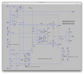
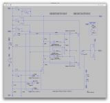
Bit hard to figure out what you have done there. The FET's look odd, one has four individual connections. Replacing the battery with a resistive load shows that little current is available. Unless I'm going cross-eyed they look to be reverse biased as well.
Bit hard to figure out what you have done there. The FET's look odd, one has four individual connections.
Yes, for me too, as I didn't come up with this. It's from someone on the ltspice newsgroup, and he's also the one who made most of the changes, like inserting those ideal diodes, changing how the X signal is made, etc...
Replacing the battery with a resistive load shows that little current is available. Unless I'm going cross-eyed they look to be reverse biased as well.
Right now I am trying to figure out the thresholds for the schmitt triggers, as none were properly setup to begin with.
As I go along, I see how un-configured triggers can interfere with the rest, so at the moment I "lifted" the output diode from one of them, and that made the X signal responsive, but I'm not even sure how it's supposed to respond, so I'm flying blind here.
I'm attaching my latest work in progress.
That sim from the other linear IC helped understand certain things a bit better.
Since the charging current remains near 2.7mA and then just drops when the "battery" voltage is high enough, I suspect this current value to be the trickle pre-conditioning one and that the lack of effect from the prog res may be due to the fact that it remains in this trickle mode without kicking in higher gear in the next charging phase of constant current. This may be only due to the un-configured thresholds.
And I'm having doubts about the lt1011. Not sure how this should work yet.
Attachments
This bit doesn't look right me. P channel FET's should be biased with the source as the most positive with respect to the drain.
You're probably right, and I'm wrestling with it without much success yet.
I didn't come up with this, and I couldn't come up with something like it anyway, so I'm just trying out suggestions. Hopefully something will come out that does work.
The other thing is the Vgs of the devices your using. Have you enough voltage available to turn them on.
I don't know. Those mosfets are the generic ones from the library and I don't know if we can override their characteristics.
I just tried something with the lt1011, using the jig that comes with ltspice and trying out a few things, I have doubt that it'll work as we have it in this simulation.
I tried it with the ground left floating as we have it, and it didn't work. I also tried it with -V tied with ground and that didn't work either.
Surely there are quite a few issues to resolve before this will work as intended.
For the mosfets, I think it might end up better with the models embedded in the asc so we can tweak them.
This bit doesn't look right me. P channel FET's should be biased with the source as the most positive with respect to the drain.
Now I'm getting serious doubts about that contraption with those mosfets at the top where the mystery box is. I just can't figure out how this works and how it's supposed to work.
The other thing is the Vgs of the devices your using. Have you enough voltage available to turn them on.
In most places it's probably not too critical because they're triggered by the outputs from those comparators, and those are all or nothing, so we have 5V to trigger those mosfets.
I found out I was not understanding correctly how those schmitt triggered buffers work, mostly the true meaning of that Vt parameter. So I've been experimenting and now I know why they were not working earlier.
But I also find that the lt1011 just won't do anything, so now I'm going to try using the same schmitt triggered comparators as the others already there, and just use 0 hyteresis to make them plain comparators. This may work better, as they don't need to be hooked up to power in the circuit and no dual supply.
I'm still reading 🙂 but have no quick answers I'm afraid. I suspect there could be quite a bit of logic (for gating and so on) within that chip that's just not shown in the block diagram.
In some ways you might be better starting from scratch and developing your own circuit that does the required basic functions. Its a major design challenge though.
In some ways you might be better starting from scratch and developing your own circuit that does the required basic functions. Its a major design challenge though.
I'm still reading 🙂 but have no quick answers I'm afraid. I suspect there could be quite a bit of logic (for gating and so on) within that chip that's just not shown in the block diagram.
Definitely! That's what I've been thinking. Quite a bit isn't shown and I also think there is probably a link between that bottom comparator for the direction control and that mystery box up there, but none of that shows.
In some ways you might be better starting from scratch and developing your own circuit that does the required basic functions. Its a major design challenge though.
I did think about that, and it is a bit too much for me, but I've been doing something in between lately, without re-designing it all from scratch, the overall structure should be usable and a bunch of stuff grafter onto it to obtain the expected behavior. Still challenging but probably more possible for me.
I have been trying to isolate most functions by disconnecting many parts and tweaked to get some of the functions behaving closer to needed. I have all of the bottom left comparators disconnected and the important ones in the middle for the pre-con, term and charge connecting as a go along. That is how I found out I was not understanding well enough how those schmitt triggers actually work, and that the lt1011 just didn't work at all.
Replacing the lt1011 by the same schmitt triggered comparators as already in there, and giving those a Vt=0 and Vh=0 makes them behave like normal comparators, and since the strobing is built-in those, it's ready to use and doesn't require power supplied, so no issues with the single supply.
Doing this allowed me to get a couple of them to finally activate and the VA/CA signals now do change state.
And this also allowed the stat signal to do something as well, but it's not yet quite right, because as I saw in the datasheet, the stat signal should be activated during all stages of charge, even the pre-con, which isn't happening in my current sim. But at least the stat signal now activates when the charge signal activate, which would be the constant current phase.
However, although that signal does now activate, the actual current going to the battery isn't the constant charge one, instead it drops progressively.
So there is definitely something wrong with all that mosfet setup that commands the Vbat.
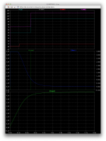
It is so odd that when the VA/CA signal steps up, because of that current source above, the voltage there steps well above the Vdd, which just isn't right.
Take a look at my screenshots. This is the latest. V(n002) is the signal from the 2 mosfets VA/CA going up to the current source and 2 other mosfets up there. More than 12V isn't quite right from a Vdd at 5.5.
V(n006) is the pre-con signal take after the diode, going between that resistor ladder. And V(n004) is just the one above that 3k9 resistor, going to the - input on the CA comparator.
It's obviously acting but not doing what's expected.
Having disconnected all of the extra stuff from below, which is just the safety stuff in case of special situations like over/under voltage or lack of Vdd, now it's down to only the 3 comparators dealing with the 3 charge phases.
And I can see now that the mosfets that should be doing the regulation are not doing it, and when I raised the Vdd from 5 to 5.5, I found out the Vbat maxed out higher than the 4.4, so that voltage isn't obtained from the regulation but from some drop out from Vdd and current flowing somewhere in a resistive path.
A lot more to do for sure.
Attachments
I couldn't figure the regulation out either. The comparator outputs to the FET's are either on or off (that's what comparator's do, they do not operate in a linear mode) and so it looks like that part of the puzzle is missing to. There would need to be some feedback mechanism to regulate the voltage and the FET's would need to be operating in a linear fashion, not just on or off.
I couldn't figure the regulation out either. The comparator outputs to the FET's are either on or off (that's what comparator's do, they do not operate in a linear mode) and so it looks like that part of the puzzle is missing to.
Definitely! And I don't see how I can make this work as is.
There would need to be some feedback mechanism to regulate the voltage and the FET's would need to be operating in a linear fashion, not just on or off.
And that's why I'm not thinking I should just start from scratch and ignore the datasheet's schematic, which is far too incomplete, and instead do just a kind of reduced behavioral model, which won't implement all of the behaviors, just the most important ones, especially the whole charging cycle.
It's not going to be easy either, but probably better in the long run than trying to figure all that was omitted from the schematic.
It really doesn't matter much what we put inside that model box (symbol), as long as it kind of behaves mostly like we need it to.
What are the goals of building a spice model of a battery control chip? For its intended application you may be better of getting a sample at testing its actions at the cases you are concerned about. If you are reusing it for some different function it may be quicker to characterize its actual performance at those cases you are targeting and then build a model to match those cases.
If you want to reverse engineer the chip there are more constructive ways to do it.
The batteries vary enough that even modeling them is a challenge with also the need to model fresh vs. worn out batteries.
I think what you are doing is interesting but may be the hard way to a simple goal.
If you want to reverse engineer the chip there are more constructive ways to do it.
The batteries vary enough that even modeling them is a challenge with also the need to model fresh vs. worn out batteries.
I think what you are doing is interesting but may be the hard way to a simple goal.
What are the goals of building a spice model of a battery control chip? For its intended application you may be better of getting a sample at testing its actions at the cases you are concerned about. If you are reusing it for some different function it may be quicker to characterize its actual performance at those cases you are targeting and then build a model to match those cases.
I'm not interested in that single chip alone, and since those are smt and there are apparently no usable chips in dip cases, I couldn't even try to test this. There is no way to breadboard this stuff, especially not for me, it's far too tiny. I couldn't even attempt to solder those things any more. That is one major thing I have against those tiny chips, they're not for the casual hobbyist.
But I have no choice, as I haven't found any that are suitable. Even that chip is lacking one feature that I do need, the handling of a load on the battery.
So I am adding extra circuitry around that chip to be able to handle the load and properly switch to the battery when there is no power coming in.
If you want to reverse engineer the chip there are more constructive ways to do it.
Nope! No reverse engineering goals here. Just design something that needs to include a button battery and its charger, among other things.
The batteries vary enough that even modeling them is a challenge with also the need to model fresh vs. worn out batteries.
I'm not trying to fully model batteries and chargers, just the behavior.
I think what you are doing is interesting but may be the hard way to a simple goal.
It would certainly be a whole lot easier if that model was already available.
What I'm designing has a lot more than just this battery and its charger. And I just need to have the behavior implemented so it can interact with the rest of the stuff.
That is why I have been thinking lately about just simplifying and make a basic behavioral model, which would not implement every single feature, just the charging cycle would be ok, with the proper handling of the power loss from the mains.
i see what you are up against. Most chip vendors do have demo boards. Its really hard to sell a complex chip without one. The demo board for this guy is Product Search and around $40.
Looking at the datasheet it seems you can use this guy to charge an LI battery, (a small one) but the load is connected to the battery not to this chip. it looks like one for their Bluetooth headset chips. Microchip is way behind in those markets. CSR has all this and everything else in one chip. But Microchip is spending big to catch up, which probably means some of this small stuff will disappear.
Typically you will have a switch mode converter tied to the battery that powers the load. TI has a typical implementation here: BQ25872 | Battery Charger IC | Battery Management Products | Description & parametrics however its 3 chips. It will charge at high current and power most typical device type loads. Its probably going the wrong direction for your task. But reading over the guide for its demo board may give some fresh insight into solving your problem: BQ25872 Complete Charger Evaluation Module - BQ25872EVM-813 - TI Tool Folder
i see what you are up against. Most chip vendors do have demo boards. Its really hard to sell a complex chip without one. The demo board for this guy is Product Search and around $40.
I can't be breadboarding everything in the design. It's the main purpose of simulations, to avoid having to do too much that way. The cost is too high and this would be only for one small function in a much larger design.
What I need is very basic and the part count doesn't need to add up.
That chip is missing the load handling feature, besides not being through-hole, so I'm forced to add a few parts around it, just to be able to do the missing feature, and I don't even know exactly yet how the issue of the smt will be handled.
This is for a diy build, and personally I am unable to handle any smt or tiny stuff, so I'm doing all I can to select parts that I can manually handle.
Looking at the datasheet it seems you can use this guy to charge an LI battery, (a small one) but the load is connected to the battery not to this chip. it looks like one for their Bluetooth headset chips. Microchip is way behind in those markets. CSR has all this and everything else in one chip. But Microchip is spending big to catch up, which probably means some of this small stuff will disappear.
Too much stuff becomes obsolete much too fast. We always have to keep up and it's a pain.
I don't need this for bluetooth or usb, and I don't need this kind of complexity. The only complexity is to properly charge a small coin cell (2032), and the load must always remain powered.
That charger isn't made to handle the loaded cell. It would throw off its proper charging cycle.
All I need is a tiny load, just a few microamps, and the battery should be able to last for many months on a charge if it gets no power for some time.
Typically you will have a switch mode converter tied to the battery that powers the load. TI has a typical implementation here: BQ25872 | Battery Charger IC | Battery Management Products | Description & parametrics however its 3 chips. It will charge at high current and power most typical device type loads. Its probably going the wrong direction for your task. But reading over the guide for its demo board may give some fresh insight into solving your problem: BQ25872 Complete Charger Evaluation Module - BQ25872EVM-813 - TI Tool Folder
That's even more expensive and complex, plus I don't want any switch mode power supply around this stuff. I will have a tiny microcontroller there and that already has an internal clock, so some high frequencies will be around but a switch mode psu somewhere is unwelcome.
This stuff will be very close to low level audio circuitry, so I want to keep this as clean as possible, and keep the part count low. And of course, keep it diy friendly.
I'm not locked on microchip specifically, and I've been digging through all kind of sources and manufacturers, hoping to find a DIP6 or DIP8 part that will do exactly what this MCP chip does, plus handle the load, but there aren't any.
So I have no choice but to do some hybrid, and I'll have to figure out how this tiny smt chip will be integrated in the rest which will all be through-hole, except probably also the microcontroller, although I may use a pic12fxxx which does come in DIP.
This looks to address what you need: http://cds.linear.com/docs/en/datasheet/4071fc.pdf Its designed for small batteries. It will feed the load from the battery. It has all the charge management you need and the small charging current you need for a small rechargeable button cell. A non rechargeable cell will not be happy there so make sure the right cell goes in. Its in both a small leaded package and an "impossible for humans" package.
With mobile electronics like cell phones being the dominant products these impossibly small packages are the wave of the future.
A quick check of the capacities of coin cells confirms that its not much: http://www.mouser.com/ds/2/88/RJD_series-962351.pdf The biggest is 150 mA w/ 1A peak. That's a 500 mA/H cell, larger than the one you mentioned. The LT chip should work OK for it. I'm not sure what the load for the cell is so i can't help much more. I know this is a whole specialty at the IC companies and none of it is simple.
This is a nice primer on charging LI batteries: Charging Lithium-Ion Batteries ? Battery University and info on extending the life: How to Prolong Lithium-based Batteries - Battery University
I'm still here but unable to add much I'm afraid.
Have you had a good look through all that LT offers ? Try ticking the 'power path ' option as well.
Battery Management - Linear Technology
Have you had a good look through all that LT offers ? Try ticking the 'power path ' option as well.
Battery Management - Linear Technology
- Home
- Design & Build
- Software Tools
- Spice simulation