Well the FET asc did run OK in my copy of LT IV so the model is there (in Windows anyway) .
I thought it should be, no matter the platform, I suspect the library remains the same. But that generic mosfet may or may not be suitable. The rest of it remains uncertain.
I had a quick look at your file... it wont be easy I suspect. The LT1011 comparator might be worth a look as it has a strobe input that is active when pulled down to ground via a suitable resistor (not a direct connection).
I thought it wouldn't be easy, but I need this and I'd like to make this work. And it would be shared, so help others too.
That LT1011 would be instead of the lm311 right?
Was I correct to assume that it's a plain buffer with strobe that commands those mosfets for that stat output?
That too probably needs tweaking to make sure it works as intended.
In that asc file, I only put parameters in one of the schmitt triggered comps, and the values are arbitrary, so probably won't work as is.
Yes instead of the LM311, and the LT1011 looked sort of suitable because it has a strobe and of course its in the library. I wonder if the buffer has an inhibit or strobe to put the status output in an 'open' condition depending on the inputs to it of course. Like tristate logic.
Yes instead of the LM311, and the LT1011 looked sort of suitable because it has a strobe and of course its in the library.
I just tried this, and wow! That thing has 3 extra signals instead of 1, for that whatever strobe is. So I just grabbed a datasheet and I'll have to figure out how this works.
I wonder if the buffer has an inhibit or strobe to put the status output in an 'open' condition depending on the inputs to it of course. Like tristate logic.
In the 832 version, only one of the mosfets are there on that stat output, but the 831 has both, so that pretty much makes it tristate capable.
And that extra signal on the buffer driving those mosfets has to be something like that, an inhibit seems logical, but I'm not sure what it would do when it's not enabled, put the output in tristate? With the 2 mosfets, that signal should go either up or down, and then also tristate I must assume. This would not hold for the 832 with only one mosfet, which would be like an open drain only.
After looking at the LT1011 datasheet, I have doubts that it can be suitable, because it is made for dual power supplies, with the ground, and not a single, so since everything else inside that MCP chip is single power supply, I don't see how this would work. The output from that comparator would want to drop below zero, if it could, but it couldn't because there isn't a dual supply for it.
The comparator should be workable. The status indicator I would worry about later, aim to get the basic functions working first.
I think you connect ground and the minus supply pins together for single rail. Try it in a simulation and see how it performs.
I think you connect ground and the minus supply pins together for single rail. Try it in a simulation and see how it performs.
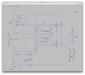
I had to rearrange a few things and reroute, but it's in there.
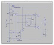
The thing is, this schematic isn't complete yet, as it's still missing a small but important part near that top mosfet (highlighted), the direction control, which remains a mystery for now.
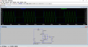
I tried running it, with a 5V dc supply, but the stat signal is up and the vbat sends power to the battery, but I'm not certain my little test contraption on vbat with the R/C as a battery is going to be suitable. I tried with different values, but everything stays pretty much static.
I tried giving it a "pulse" instead of dc power for the whole circuit, starting with no power at all, and after a short time, turning it on, and there goes the stat and vbat, the same as if dc powered from the start.
I figured a large cap with a resistor would kind of simulate a discharged battery at first, then as the big cap charges, it would behave like a charging battery, using the R/C constant like a charging curve. But I'm not seeing any hints that it would happen.
But again, this thing is missing that direction control piece, which might/should make a difference.
Attachments
Could the direction thing be a solid state relay that passes current in either direction irrespective of polarity ?
I really haven't got a clue about what that mystery box could contain, but I assume if it had more mosfets, that those would be drawn as the others in the schematic and not put away in a box with who knows what else. It would stand to reason that there aren't any more mosfets to this schematic than there are already and that whatever is in that box would rather be something that commands those 2 mosfets below. Those that we see in the schematic.
What I see about that box, is that it has 3 connections, one to get power from Vdd, an other "senses" Vbat, and the last one seems to go to the gate on the mosfet below.
However, I do see something odd about that particular connection: that mosfet already has a gate that is connected to the line below, along with the other mosfet's gate, which to me means they are commanded by the same signal, but although that 3rd connection from the direction control box seems to be going to the mosfet's gate, I can't be certain it's the same gate as the one going down to the line below.
Plus that mosfet seems different from the others, not only doesn't it have a schottky diode across it, it doesn't have the connection between those 2 legs at the source.
Something is odd there, and I have no clue about what is going on.
This is the missing part for this model, and I don't think it can work without it, so until something can be figured out, it can't truly be tested.
I don't even understand how there could be bi-directional currents there, as it's hooked up to Vdd and current could only come from there and not the other way around. Am I missing something?
Block diagrams, or basic circuit/block diagrams can be very simplified compared to what is actually in there.
This is Li-On do-dah isn't it. Doesn't that mean the (user) load is not connected across the battery but connected to the other side of the chip. The chip monitors current in and current out of the battery. No ? yes 🙂
If it did work like that then it might make sense to have some kind of bi directional switch in there that could also isolate the battery if needed from the either the charge current or the load.
I've never studied these things so I'm just basing that on scanty knowledge I've picked up.
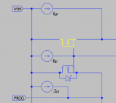
The way I did it doesn't really match the datasheet schematic.
I just dropped a generic pmos there, the same as the one below, but we can see that this isn't what's actually there in the datasheet schematic, at least not quite.
And the difference isn't just the lack of the schottky, there is something more, not to mention that mystery box.
I'm stumped!
I just dropped a generic pmos there, the same as the one below, but we can see that this isn't what's actually there in the datasheet schematic, at least not quite.
And the difference isn't just the lack of the schottky, there is something more, not to mention that mystery box.
I'm stumped!
Attachments
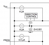
Looking at that and the mystery box could perhaps get some logic input from elsewhere in the device to control the current flow.
I don't know.
I don't know.
Block diagrams, or basic circuit/block diagrams can be very simplified compared to what is actually in there.
Sure, but why have mosfets all over and then keep out a couple of them in some box?
And if there was some type of dual mosfet SSR in that box, why would it come in parallel with one more mosfet? the one below that box.
This is Li-On do-dah isn't it. Doesn't that mean the (user) load is not connected across the battery but connected to the other side of the chip. The chip monitors current in and current out of the battery. No ? yes 🙂
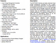
Yes, it's a battery charger, and I haven't seen any mention of any load on the battery, so far. That charger just charges the battery and isn't meant to handle any extra load on it while it's charging. A load while charging would throw off all the charging protocol (constant current, constant voltage), so this charger isn't meant to have the load present on the battery while charging it, which is one reason for me why this circuit by itself isn't quite suitable for my needs, and I need to add more stuff around it to handle that load.
If it did work like that then it might make sense to have some kind of bi directional switch in there that could also isolate the battery if needed from the either the charge current or the load.
Where would the load be connected? It can't be loading the battery while the charging occurs.
I've never studied these things so I'm just basing that on scanty knowledge I've picked up.
Neither did I, and I'm discovering things as I go along.
I've been trying to find the right kind of IC to handle what I need in a design, but couldn't find any 100% suitable, so this one is the closest to meeting my needs.
Although it does have one huge issue for me, it doesn't come as a through-hole part, only smt, and that's one issue for which I have no solution yet.
I really need to find one like it, with ability to handle the load live during charging, and be a through-hole part. A 5 legged critter that eludes me.
Looking at that and the mystery box could perhaps get some logic input from elsewhere in the device to control the current flow.
I don't know.
That was my thinking as well. I don't know what it is, but I suspect some kind of logic to command those mosfets below. Both of them, since they have their gates hooked up together, but perhaps the one right below that box flows the other way, but can't tell from that schematic, since it's missing the schottky and there is no connection that would show on which side the source is.
What I really would want to find is a "normal" (PDIP8) IC, with the same features as this one, plus the ability to handle a load at the same time.
But for now, I want to try to make this one work.
One thing that was eluding me was from the feature list in the datasheet. Which is the ability to select choices for pre-conditioning and end-of-charge, but this seems to be done by choosing the right variant of the chip and isn't done by electronics around the chip.
Only the charging current is chosen by the external resistor on the prog pin.
One thing I also noticed in the datasheet but that doesn't show explicitly in the internal schematic, is the fact that there is a thermal sensing done, that affects the charging, so I guess putting the chip as close as possible physically to the battery being charged makes this whole thing better.
Attachments
I just re-read through the whole datasheet, in the hope of finding some details that would provide some hints at how this thing works inside.
But it's obvious there is a whole lot more going on inside that thing than we can see on the schematic.
That schematic is highly simplified and omits many things.
For one thing, obviously there are several current sources, plus a reference voltage generator, that require many parts to implement.
Plus there are obviously a few protection parts, like diodes, to protect against reverse hookups. None of that represented.
Nothing is represented for all the thermal protection and regulation.
The parts do come in many "variants" to provide those different configurations for preconditioning, end-of-charge and various currents and voltages, for example the regulation voltage (charging voltage), which is chosen by a part variant being "programmed" at the factory.
I'm assuming some of those programmable variants are done at the factory by adjusting the values of the resistors on that schematic, but I suspect there is more to it, not shown.
This schematic is closer to a synoptic diagram than a real full schematic. Many things not shown.
For a simulation, we don't really need all the details, as we can use current sources and voltage source for references, but we do need to know what those mystery boxes actually do, so we can use something to emulated the wanted behavior.
I have not seen anything in the datasheet giving enough details to know what's inside that mystery box.
I do suspect it may have something to do with the UVLO (Under Voltage Lockout) and the battery detection and its voltage (when overly low, deeply discharged).
But how does it actually work? Dunno!
I wonder if the mystery box could be some low drop out programmable constant current source. Thinking about it, if it were just a FET or as I perhaps thought a bi-directional type of relay then that would connect the battery to the incoming voltage with no current limiting.
Not easy to suss out at all.
Not easy to suss out at all.
I wonder if the mystery box could be some low drop out programmable constant current source.
If there is a current source in that box, why would they draw just a box and not the current source? Unless they are doing this purposely to blurr things up a bit.
They have drawn explicitly a bunch of other current sources, so why would they hide one more? We can only speculate for now.
Thinking about it, if it were just a FET or as I perhaps thought a bi-directional type of relay then that would connect the battery to the incoming voltage with no current limiting.
Same as with a current source, if they draw all the mosfets but not those in that box, would that just be a way to obfuscate things? or just that what's in that box is something else?
For one thing, if there were a couple more mosfets inside that box, as some type of switch, then it would come in parallel with the mosfet that is shown below. Would that make any sense?
Now that makes me wonder one more thing, let's say the contents of that box is some kind of command logic, maybe getting its parameters/info from some other parts inside that chip, and that it commands that shown mosfet right below it, and I suppose maybe both of those mosfets, if the gate signal goes down to where both mosfet's gates are connected, then perhaps that logic in that box is what does commands those 2 mosfets.
And one more thing, that mosfet right below the box, looking a bit different from the others (no schottky for one thing), could be a simplified representation of some arrangement, perhaps of 2 mosfets instead of one, arranged as a bidirectional switch...
I still don't understand how it really could be bidirectional, with current flowing back up towards the Vdd. I must be missing something...
Not easy to suss out at all.
Quite right. And I didn't realized when I started with this how it could be so difficult.
I am trying to see what I can find out with the ltspice yahoo group. More people are ltspice gurus in there, and I'm hoping some will have some insight and unlock some clues.
No easy answers to all that I'm afraid.
If you know how the device works and behaves in a given application then it might be more successful to design your own circuit from scratch to meet those requirements. No doubt there is a lot going on inside the chip though as quickly reading a bit on Li-On charging suggests that the charger will switch from constant current to constant voltage at some predetermined point, and then stay in CV mode only for a certain time before terminating the charging.
If you know how the device works and behaves in a given application then it might be more successful to design your own circuit from scratch to meet those requirements. No doubt there is a lot going on inside the chip though as quickly reading a bit on Li-On charging suggests that the charger will switch from constant current to constant voltage at some predetermined point, and then stay in CV mode only for a certain time before terminating the charging.
No easy answers to all that I'm afraid.
Unfortunately true, as I'm finding out.
If I could understand better how it works as drawn, maybe it might be possible to infer more details. I'm stumped at present. But maybe, hopefully, something will come up. I'm sharing this with more people on other forums.If you know how the device works and behaves in a given application then it might be more successful to design your own circuit from scratch to meet those requirements.
Overall yes, that's how it works, with a little more to it for the condition when the battery is deeply discharged, with an overly low voltage, then before going into normal charge cycle starting with the constant current, it first goes into a trickle mode until a voltage threshold is reached. That threshold is hardwired at the factory as a percentage of what we set on the prog input.No doubt there is a lot going on inside the chip though as quickly reading a bit on Li-On charging suggests that the charger will switch from constant current to constant voltage at some predetermined point, and then stay in CV mode only for a certain time before terminating the charging.
And of course there is some handling for reversed battery, non-present battery, etc...
But I guess for a simulation with proper behavior, we don't even need all those features, all we need is the charging cycle, or facsimile.
I just found out I had already made a few mistakes in what I did, from that ltspice forum. I had switched some mosfets at some point, and since I'm using the library generic ones without their schotty associated, when I put them in place they were reversed.
I'm posting an updated screenshot.
And there is one more thing I'm wondering about: on their schematic, it shows a G=0.001 near the second mosfet from the top, below that direction control box. What do they mean by that?
Attachments
- Home
- Design & Build
- Software Tools
- Spice simulation