Rule of thumb for class A amps is you should be able to comfortably keep your hand on the heatsink for ten seconds. 44°C is certainly fine.
For future reference, in regard to the method of lifting resistor legs that you're mentioning (which I totally forgot about):
If both(!) R19 and R20 are disconnected from the circuit by lifting one leg, the IRFP240/9240 will not turn on, meaning that no current will pass through the output stage. The IRFP240/9240 do not conduct without a voltage present at the gates (normally off type, look at the Vgs-Id charts in the datasheets, they need a few V to turn on). With R19/R20 removed, the mosfets stay off, no current will pass. This allows biasing of the frontend and setting the bias voltage for the output stage.
If you look through the thread, you'll find that consensus is 50mV to 200mV. It will change with temperature.
Of course. Im just finishing the pre amp (Ba3) and other thing. Its been a 5 year long building and tuning process, part of a catharsis i've been through. I was thinking of sharing the whole experience in a dedicated post with some explanations. The system is a dual mono, dual amp, pre amp, RIAA, open baffle pure audio like. So, a lot of images to come
if feading the vfet with a ba3 pre amp, what harmonics should we have? Do we nule the H2 or make it equal to H3? Or make H2 dominant? Is there a logical way of doing this? i am thinking that if maybe, nuling the harmonic distortion at the Ba3 would make the power amp to give the colours it has. Other way, we are just adding colours that are not meant to be there. Just thinking. What are your insights? thanks
You're at a point where you can tailor the sound to your liking. Try all the configurations you mentioned, see what tickles your fancy, that's what BA3's P3 is for after all 🙂
I have ordered the boards from the DIY store, but have been unable to find a BOM. I have attempted to write one. Could one of you gentlemen point out my errors please? Thanking you in advance.
View attachment Sony VFET BOM.pdf
View attachment Sony VFET BOM.pdf
Here's the original BOM from the Supplemental Kits that were created awhile back:
Here is the corrected BOM, the previous one has been deleted..
Sorry for making your lives difficult! Especially secanbj
Attachments
I have ordered the boards from the DIY store, but have been unable to find a BOM. I have attempted to write one. Could one of you gentlemen point out my errors please? Thanking you in advance.
View attachment 877341
re your message: Matching is more beneficial to the CSX2 than the CSX1. Page 8 of the VFet part 2 guide that outlines the CSX2 quotes:
"I matched the VFETs for a Vgs within 0.1 volts at 0.5 amp current at 20 volts,and 0.2V Vgs is good enough. Some of you won't have good matches or onlyenough VFETs for 1 pair per channel, but you can build the amplifier and it willwork fine, with somewhat less power and higher distortion. I tested that with 1amp bias current, and it did just under 20 watts into 8 ohms."
I've learned there are a lot of so called VFet 'KITS' being sold which are none other than the DIYAudioStore PCBs and the 4 VFets. IMO, a kit should include ALL parts required to build the amp ; particularly the JFets.
The diyAudio Sony VFET Part 2 amplifier had an optional supplemental parts package that included all of the amplifier board parts and was sold by diyAudio Store. Power supply and chassis was supply-it-yourself.
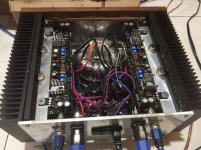
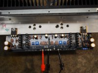
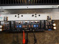
After few years in my drawer, I finally found time to finish the Sony VFET amp.
Great soundstage, very good in all areas from high, mid and tight bass.
Other than the M2, this is my new favorite, followed by the F4.
The test procedure provided by Nelson was very easy to follow.
Even with single multimeter, all went well.
Thanks a lot to Nelson's generosity.
Great soundstage, very good in all areas from high, mid and tight bass.
Other than the M2, this is my new favorite, followed by the F4.
The test procedure provided by Nelson was very easy to follow.
Even with single multimeter, all went well.
Thanks a lot to Nelson's generosity.
Attachments
Last edited:
Hi Dennis,
Spot on you were right, with the Fairchild transistors R34 & R35, I replace it with 470R to dial P3 & P4 more to 1.5Vdc.
Roland
Spot on you were right, with the Fairchild transistors R34 & R35, I replace it with 470R to dial P3 & P4 more to 1.5Vdc.
Roland
Greetings to all in the new year.
I'm trying to finish the Sony VFET I started over the summer. I have assembled and tested the resistances and all are OK. But am having a problem with a couple voltages.
At this point, everything is installed except the VFETs.
I am using LSK170 and LSJ74 - both grade C. They were not matched. The K170 were about 11mA Idss and the J74 >12mA (according to DCA75). I have K2013 and J313 for Q6 and Q5.
All voltages test fine except the following:
Left Channel:
T6-T7 = 8.7
T8-T9 = 8.7
T6-T11 = 11.3
T8-T13 = 11.3
T18-Gnd = 9
Right Channel:
T6-T7 = 8.2
T8-T9 = 8.2
T6-T11 = 10.7
T8-T13 = 11.2
T28-Gnd = -16
Also - only right channel - T4-Gnd = -2.7
P3 and P4 are set fully CCW - turning them only makes it worse.
I'm assuming this is caused by JFETs with too high Idss but I don't know what I should do about this. I do have other JFETS and can probably find a matched set.
All ideas appreciated.
Attachments
You have a lot of current running through Q5 and Q6, likely caused by the Idss of
the jfets and R34/R35 values.
Please confirm the part values you have for R34, R35, P3 and P4.
I expect you will need to reduce R34 and R35, perhaps to 100 ohm.
The T18-Gnd values just represent the current imbalance between Q5 and Q6 for don't
worry about that for now.
the jfets and R34/R35 values.
Please confirm the part values you have for R34, R35, P3 and P4.
I expect you will need to reduce R34 and R35, perhaps to 100 ohm.
The T18-Gnd values just represent the current imbalance between Q5 and Q6 for don't
worry about that for now.
Thanks, Dennis.
R34 and R35 are both the stock value - 221 ohm
P3 and P4 are also stock 500 ohm
I do have some JFETs with lower Idss. Is that the next step or can I resolve with different R34/35 and P3/4 values?
Also do I need to worry about T4 - Gnd = -2.7V at this point?
Cheers.
R34 and R35 are both the stock value - 221 ohm
P3 and P4 are also stock 500 ohm
I do have some JFETs with lower Idss. Is that the next step or can I resolve with different R34/35 and P3/4 values?
Also do I need to worry about T4 - Gnd = -2.7V at this point?
Cheers.
- Home
- Amplifiers
- Pass Labs
- Sony vFET Illustrated build guide