You may need to increase R34 and R35 to get them to bias correctly as the VGS is higher on the Fairchild parts.

another quick question. ztx550 appears to be obsolete. what can be used as an alternative? Many thanks
Couls simply ztx551/451 be used instead? From what I can gather from the data-sheet they are almost identical
The brackets must be flat against the heatsink with thermal grease and torqued properly to ensure maximum thermal transfer.
What would be the appropriate torque value for bracket-heatsink coupling?
I have now tested DC voltages across the test points and compared to the 2nd chart in Pa's documentation. Most values are OK, except the ones below.
Q5 and Q6 are Toshiba parts. Should I decrease R34/35?
G-T19 = +22V (instead of +12V)
G-T20 = -22V (instead of -12V)
G-T17 = -17V (instead of -10V)
G-T16 = +19V (instead of +10V)
How critical are those values at this stage?
G-T18 is 5V in one channel and only increases turning P3. The other channel is 1V.G-T18 This may initially read very different than 0. If so, make a small adjustment to P3 and set until it reads +/- 1.0v
Q5 and Q6 are Toshiba parts. Should I decrease R34/35?
Here both channels differs more than 4V:G-T19 , G-T20, G-T17, G-T16 The suggested voltages are very rough. Within 3-4 volts is fine.
G-T19 = +22V (instead of +12V)
G-T20 = -22V (instead of -12V)
G-T17 = -17V (instead of -10V)
G-T16 = +19V (instead of +10V)
How critical are those values at this stage?
I'm in the process of building my unit. I wanted to ask if there's been, among the many units build, any failure ( primary or secondary) of the vfets ( without building mistakes) to understand what could be the potential expected life of the amplifier and if it would make sense to try to acquire some extra vfets as future replacements.
Thanks
Benjamin
Thanks
Benjamin
I haven't followed all the discussions of this project, but I don't recall seeing mentions of vfet failures; I personally wouldn't worry too much about it.
Also Papa has commented in the past that the Sony devices are pretty rugged.
While generally it's a not a bad idea to have spare devices around, but please be mindful of the fakes out there.
Have fun with your build.
Dennis
Also Papa has commented in the past that the Sony devices are pretty rugged.
While generally it's a not a bad idea to have spare devices around, but please be mindful of the fakes out there.
Have fun with your build.
Dennis
There have been no failures that I'm aware of. Just follow the build guide exactly and you shouldn't have any problems. If I can do it, just about anyone can!
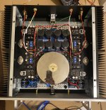
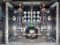
I have know completed my build. I’m still bench running it. Construction was without any issue. The goop was probably the most painful part. Testing and initial set up also went smoothly.
The amplifier has been running know for a couple of hours. Output dc offset is stable at under 10mV and so is the voltage drop between T1 and V- at around 100mV. Dc offset at T18 is around 50mV. I just get some drift on T6T7 and T8T9. They stay at 1.5v without the lid but after one hour of operation with the lid on they Were at 1.53v. Is this acceptable or should I turn them slightly down?
The amplifier has been running know for a couple of hours. Output dc offset is stable at under 10mV and so is the voltage drop between T1 and V- at around 100mV. Dc offset at T18 is around 50mV. I just get some drift on T6T7 and T8T9. They stay at 1.5v without the lid but after one hour of operation with the lid on they Were at 1.53v. Is this acceptable or should I turn them slightly down?
Attachments
Congratulations on the nice build! I wouldn’t worry about such a small drift.
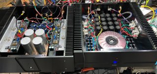
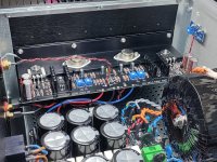
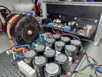
Is the green wire coming from the RCA a second ground return? Just curious if it's addressing a specific issue.
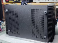
Not a functional mod, but I’d consider adding some heat-shrink tubing around the mains power inlet tabs/wires - just as a safety precaution. You never know when poking around inside the amp. ⚡
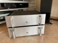
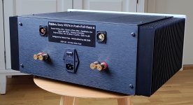
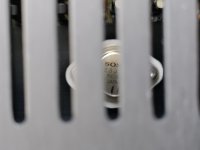
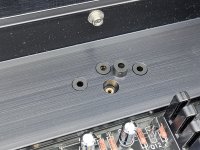
A picture of the front panel would be appreciated - I am thinking to add handles to my next project as well. 👍
Is the green wire coming from the RCA a second ground return? Just curious if it's addressing a specific issue.
Not a functional mod, but I’d consider adding some heat-shrink tubing around the mains power inlet tabs/wires - just as a safety precaution. You never know when poking around inside the amp. ⚡
A picture of the front panel would be appreciated - I am thinking to add handles to my next project as well. 👍
Thanks!
You are right about the shielding of the 220v terminals but know I would have to desolder everything and at this point I’m just to lazy😅
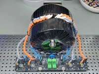
The green cables are the ground connection of the shielding of the signal cables. I already had them and used them. Probably pointless but didn’t want to leave the shielding unconnected.
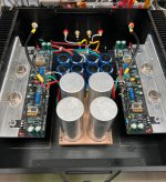
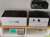
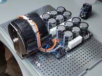
Attached a frontal view (above the vfet, below a dual mono F4)
You are right about the shielding of the 220v terminals but know I would have to desolder everything and at this point I’m just to lazy😅
The green cables are the ground connection of the shielding of the signal cables. I already had them and used them. Probably pointless but didn’t want to leave the shielding unconnected.
Attached a frontal view (above the vfet, below a dual mono F4)
Attachments

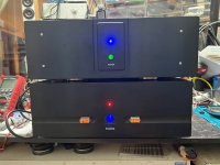
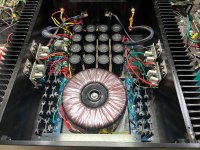
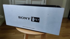
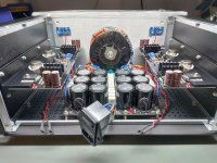
My Sony VFET Push-pull is finally singing. I am late to the game, but just in time for this year’s birthday. 🎁
It’s been a fun journey chasing all the unobtanium components across three continents, and following Nelson’s documentation along with Jim’s excellent circuit explanations.
Many people helped through private conversations — thank you all! A special mention goes to Charles, sadly no longer with us, whom I had the pleasure of getting to know thanks to this very special project. 🙏
Attachments
-
 2025-06-08 10.41.34.jpg705.6 KB · Views: 83
 -
 2025-06-11 08.34.13.jpg369.7 KB · Views: 79
 -
 2025-06-11 08.35.04.jpg189.7 KB · Views: 79
 -
 2025-06-11 08.36.36.jpg170.5 KB · Views: 81
 -
 2025-06-11 08.48.02.jpg293.7 KB · Views: 83
 -
 2025-06-08 10.39.06.jpg688.3 KB · Views: 79
 -
 2025-06-03 17.58.16.jpg528.2 KB · Views: 83
 -
 2025-06-03 17.34.29.jpg551.8 KB · Views: 76
 -
 2025-06-02 17.54.25.jpg823.6 KB · Views: 68
 -
 2025-06-02 16.12.36.jpg591 KB · Views: 70
 -
 2025-04-03 16.59.38.jpg669.9 KB · Views: 73
 -
 2025-03-04 17.33.07.jpg722.1 KB · Views: 74
 -
 2025-02-28 17.39.05.jpg562.3 KB · Views: 76
 -
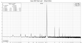 2025-06-09 - Sony VFET Push-pull - FFT.png117.5 KB · Views: 81
- Home
- Amplifiers
- Pass Labs
- Sony vFET Illustrated build guide