you certain of good orientation of Q11 and Q12?
if yes , fiddling with P1 and P2 must get you in ballpark , regarding T19 and T20 voltages
that will sort T16 and T17 also
Perfect! Adjusting P1 and P2 made all voltages perfect!
Regards,
Dan
well , I had suspicion from the start ( of the thread ) that they (trimpots) are there exactly for purpose of trimming voltages
it seems you helped me to solve that suspicion

take care of reading entire start-up procedure over and over , until you're sure of grasping things ....... because you evidently had luck on your side , to this stage
when you have VFets in circ , there is no place for luck
it seems you helped me to solve that suspicion
take care of reading entire start-up procedure over and over , until you're sure of grasping things ....... because you evidently had luck on your side , to this stage
when you have VFets in circ , there is no place for luck
Last edited:
well , I had suspicion from the start ( of the thread ) that they (trimpots) are there exactly for purpose of trimming voltages
it seems you helped me to solve that suspicion
take care of reading entire start-up procedure over and over , until you're sure of grasping things ....... because you evidently had luck on your side , to this stage
when you have VFets in circ , there is no place for luck
I'm following the guide 'within reason'. I won't put the VFETs in until everything is perfect in the guide up to that point. So far so good. All the resistances matched the guide so then I moved to step II where all the voltages (except the supply was 31VDC) matched within a certain range.
More tomorrow.............
Regards,
Dan
Can anyone tell me if the blue leds should light before adding the Vfets? mine won't
Mine do.
Regards,
Dan
As Zen Mod has suggested,
Here's the details.
Both my boards passed the PART 1 TESTING THE RESISTORS with flying colors.
Now Part 2- APPLYING THE POWER TO THE FRONT END
Everything appeared to power up well with no smoke so I was happy. I went through all the initial voltage test points and everything looked good until I got to G-T19 and G-T20. They were 24V each. Also, G-T17 and G-T16 were 20V. After a little coaching from Zen Mod I found that I left all four pots fully CC instead of just P3 and P4. After tuning P1 and P2 my voltages returned to they should be.
Here's the latest measurements.
G-T6=31.43V G-T8=31.43V
G-T4=24V G-T2=24V
T6-T7=0V T8-T9=0V
T6-T11=5.76V T8-T13=5.69V
G-T18=0V
G-T14=15V G-T15=15V
G-T19=12V G-T20=12V
G-T17=9.9V G-T16=9.9V
Now herein lies my problem. P3 and P4 have no real effect on T6-T7 and T8-T9. Max I can get is .2V on each. G-T18 goes way up when I do this.
My first two guesses are that I damaged something by leaving P1 and P2 fully CC? Or, I may have to adjust some resistor values for higher than expect rail voltages?
Regards,
Dan
because you evidently had luck on your side , to this stage
Here's the details.
Both my boards passed the PART 1 TESTING THE RESISTORS with flying colors.
Now Part 2- APPLYING THE POWER TO THE FRONT END
Everything appeared to power up well with no smoke so I was happy. I went through all the initial voltage test points and everything looked good until I got to G-T19 and G-T20. They were 24V each. Also, G-T17 and G-T16 were 20V. After a little coaching from Zen Mod I found that I left all four pots fully CC instead of just P3 and P4. After tuning P1 and P2 my voltages returned to they should be.
Here's the latest measurements.
G-T6=31.43V G-T8=31.43V
G-T4=24V G-T2=24V
T6-T7=0V T8-T9=0V
T6-T11=5.76V T8-T13=5.69V
G-T18=0V
G-T14=15V G-T15=15V
G-T19=12V G-T20=12V
G-T17=9.9V G-T16=9.9V
Now herein lies my problem. P3 and P4 have no real effect on T6-T7 and T8-T9. Max I can get is .2V on each. G-T18 goes way up when I do this.
My first two guesses are that I damaged something by leaving P1 and P2 fully CC? Or, I may have to adjust some resistor values for higher than expect rail voltages?
Regards,
Dan
Hi Dan,
What values pots are P3 and P4 and what mosfets are you using for
Q5 and Q6? Are you using Toshibas or Fairchilds?
Dennis
What values pots are P3 and P4 and what mosfets are you using for
Q5 and Q6? Are you using Toshibas or Fairchilds?
Dennis
Hi Dan,
What values pots are P3 and P4 and what mosfets are you using for
Q5 and Q6? Are you using Toshibas or Fairchilds?
Dennis
Followed the attached PDF to the letter.
Regards,
Dan
Attachments
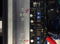
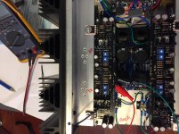
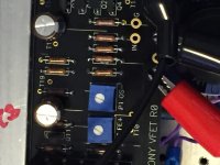
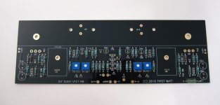
I've been reading other posts where increasing R34 and R35 are necessary? Also, I'm looking for a pic of a bare board so I don't have to guess where R34 and R35 are.
Attachments
Last edited:
can't help with that ..... my (bare) pcbs are 1km away from me and I'm lazy to stare at pcb pictures
can't help with that ..... my (bare) pcbs are 1km away from me and I'm lazy to stare at pcb pictures
No problem.

Hi Dan,
I think you can go by Papa's document:
http://www.firstwatt.com/pdf/art_diy_sony_vfet.pdf
Page 5 shows the silkscreen of the PCB.
Dennis
I think you can go by Papa's document:
http://www.firstwatt.com/pdf/art_diy_sony_vfet.pdf
Page 5 shows the silkscreen of the PCB.
Dennis
Dan, please also measure and post the voltages across R34 and R35 as suggested
by Zen Mod. That'll give an idea of the current through the jfets and
how much you need to increase R34 and R35 to get the needed voltage for
the mosfets.
by Zen Mod. That'll give an idea of the current through the jfets and
how much you need to increase R34 and R35 to get the needed voltage for
the mosfets.
Dan, please also measure and post the voltages across R34 and R35 as suggested
by Zen Mod. That'll give an idea of the current through the jfets and
how much you need to increase R34 and R35 to get the needed voltage for
the mosfets.
Many thanks to both Zen Mod and Dennis. 1.8V across both.
Regards,
Dan
1V8/220R=appr. 8mA , which is good
now , be sure that you dial back both P3 and P4 , replace R34 and R35 with , say , 390R-430R and try biasing mosfets again
check for P3 : upper leg of R35 and T10 , ohmmeter must read 0
check for P4 : upper leg of R35 and T12 , ohmmeter must read 0
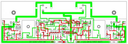
"upper leg" when looking at pcb as shown in post #755
now , be sure that you dial back both P3 and P4 , replace R34 and R35 with , say , 390R-430R and try biasing mosfets again
check for P3 : upper leg of R35 and T10 , ohmmeter must read 0
check for P4 : upper leg of R35 and T12 , ohmmeter must read 0
"upper leg" when looking at pcb as shown in post #755
1V8/220R=appr. 8mA , which is good
now , be sure that you dial back both P3 and P4 , replace R34 and R35 with , say , 390R-430R and try biasing mosfets again
check for P3 : upper leg of R35 and T10 , ohmmeter must read 0
check for P4 : upper leg of R35 and T12 , ohmmeter must read 0
"upper leg" when looking at pcb as shown in post #755
Both are exactly as you posted.
Regards,
Dan
- Home
- Amplifiers
- Pass Labs
- Sony vFET Illustrated build guide