Mr. Pass 😎
may I ask you why you choose in the design the input impedance of the output stage so low?
As you wrote a bit under 1KOhm……at least that is the value the front end output sees…...
Thanks!
may I ask you why you choose in the design the input impedance of the output stage so low?
As you wrote a bit under 1KOhm……at least that is the value the front end output sees…...
Thanks!
Last edited:
I believe loading coming from OS itself is sort of variable in nature (node jumping up and down .... so bias circuit need to have impedances as low as possible ; example - take biasing of small tube or transistor vs. biiiiig tube or transistor ) , while value of R20 need to be chosen to tame/neutralize that as much is possible
so , as input impedance of OS and nature of it is result of compromise , value of R20 need to be in same range , to became dominant
that's at least how I understand it
so , as input impedance of OS and nature of it is result of compromise , value of R20 need to be in same range , to became dominant
that's at least how I understand it
Last edited:
front end board size
Hi Mike,
I already have a dual mono chassis I'm planning on using, do you know what size your front end board would be? I have to decide whether to forge ahead point to point or wait for a board.
Thanks,
Chuck
I am working at this point to produce a front end board that would be acceptable to eventually go into the diyaudiostore. The backend of it I think will come later once the dust has settled a little. This is of course if papa approves, or has nothing else in the works.
Hi Mike,
I already have a dual mono chassis I'm planning on using, do you know what size your front end board would be? I have to decide whether to forge ahead point to point or wait for a board.
Thanks,
Chuck
..........and because M2 is out of production I hope that Mr. Pass will give free sometimes the circuits and we all can share Zen Mods experience too….
🙂🙂🙂
this could be really funny 😛
Hi Mike,
I already have a dual mono chassis I'm planning on using, do you know what size your front end board would be? I have to decide whether to forge ahead point to point or wait for a board.
Thanks,
Chuck
I do not, but there is no reason to make it large. If possible, an adapter board on current output board is an option I thinkttoo. Others have PM'd interest in using as a line amp without to many mods.
I need to have a talk this weekend with 6L6 about compliance with chassis format if we want to obey that at all in this case. I think the majority will need to adapt any compliant chassis with an L-channel aluminum like in your amps. For a back OS end board, looking to do something that will use TO-3 or TO-247 for IRF's Anyways, use of a bench drill is likely.
If I want to make a balanced amp like the big Sony VFET can I just connect R24 ( 332Ohm) to the R24 of the other halve? Just like in the BBA3?
Anybody know how to connect the global feedback switch when going balanced?
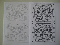
I have single layer PCB layout ready for a balanced or stereo pair, and will be etching my own boards. It's on half a 'eurocard' size ( 10 x 16 cm).
Is there a 'USAcard' size also 😀😀
I made it with a very old freeware program, LAYO1PCB, so I don't know how to share it with you...
Walter
Anybody know how to connect the global feedback switch when going balanced?
I have single layer PCB layout ready for a balanced or stereo pair, and will be etching my own boards. It's on half a 'eurocard' size ( 10 x 16 cm).
Is there a 'USAcard' size also 😀😀
I made it with a very old freeware program, LAYO1PCB, so I don't know how to share it with you...
Walter
Attachments
I do not, but there is no reason to make it large. If possible, an adapter board on current output board is an option I thinkttoo. Others have PM'd interest in using as a line amp without to many mods.
I need to have a talk this weekend with 6L6 about compliance with chassis format if we want to obey that at all in this case. I think the majority will need to adapt any compliant chassis with an L-channel aluminum like in your amps. For a back OS end board, looking to do something that will use TO-3 or TO-247 for IRF's Anyways, use of a bench drill is likely.
Would there be a benefit to having both channels of j313/k2013 fets in the row ( like the pumpkin ), as opposed to on opposite ends of the board ( like the BA-3FE? I ask only because I already have a galaxy 2u dissipante I could put this in and mounting all the matched fets to the same sink seems convenient, at first glance.
I believe loading coming from OS itself is sort of variable in nature (node jumping up and down .... so bias circuit need to have impedances as low as possible ; example - take biasing of small tube or transistor vs. biiiiig tube or transistor ) , while value of R20 need to be chosen to tame/neutralize that as much is possible
so , as input impedance of OS and nature of it is result of compromise , value of R20 need to be in same range , to became dominant
that's at least how I understand it
THX Aleksandar!
I reread the article and Nelson does not write that the input impedance of the outputstage is low, but more that the output impedance of the Frontend is low, done by R20 2k2 and the two AC loads (4k7 and 220uF going to ground too).
So the input of the outputstage sees the less 1k of the output of the inputstage.
Sorry for long version.....🙂
Nelson's is better....
"You will notice R20 which is a load to ground from the Drains of Q15 and Q16. R5, R6, R29 and R30 provide some additional AC loading to ground, and all told, the output front end sees slightly less than 1K to ground. These help set the gain of the front end along with R24, R25 and R26 and also R43/P3 with R44/P4."
And often asked.....already when noisefree asked about the 30.5 some years ago.....
Is the frontend direct coupled over the 47k to the outputstage or cap coupled over the 220uF. But these are connected over the 4k7 to ground.....:-(
Nobody else reflecting the circuit....?
and showing his ignorance...
🙂
Last edited:
it's (sort of) DC coupled over 47K , no doubt
if you calc F3 for 220uF/47K combo , you'll get where that DC coupling is becoming AC dominant
somewhere in range of 15mHz

we already chatted about DC level shifters and their overwhelming influence to sound ......
if you calc F3 for 220uF/47K combo , you'll get where that DC coupling is becoming AC dominant
somewhere in range of 15mHz
we already chatted about DC level shifters and their overwhelming influence to sound ......
I'm going to send you a bag with ,say, 100pcs of 1uF/100V Philips MKC (my fave bypass), so you'll stop taking care of DC shifting or AC coupling

do you know an answer :
http://www.diyaudio.com/forums/pass...igh-end-off-topic-thread-961.html#post4385891
?
http://www.diyaudio.com/forums/pass...igh-end-off-topic-thread-961.html#post4385891
?
I'm going to send you a bag with ,say, 100pcs of 1uF/100V Philips MKC (my fave bypass), so you'll stop taking care of DC shifting or AC coupling
....u can send me a bag as well i will make sure theygo to proper use 😉😉😉😉😉😉😛
I'm going to send you a bag with ,say, 100pcs of 1uF/100V Philips MKC (my fave bypass), so you'll stop taking care of DC shifting or AC coupling
Can you post picture from that Philips capacitor please
There is a couple (shape and size)MKC type , I would give a try as a Bypass cap.
Greetings gabor
Thank you
I do have some that type and the axial type to
I didn't knew they are such a good parts
Because they are big in size I did not tested or use them ever if my memory serve well
Greetings
I do have some that type and the axial type to
I didn't knew they are such a good parts
Because they are big in size I did not tested or use them ever if my memory serve well
Greetings
- Home
- Amplifiers
- Pass Labs
- Sony vFET Amplifier Part 2