Hello again, I built this amplifier some 6 years ago and after 2 years of listening evaluation I put it in my "prototype stock". Few days ago I got an idea how to improve mains frequency components S/N by changing just one track on the PCB - the signal GND track. And it has worked very well.
The amp uses modified output stage from ExtremA by Sander Sassen which was put in the loop of a good opamp. The output stage uses local NFB and has vanishingly low distortion below 0.001% itself, but quite high output impedance of 0.235 ohm. In the opamp feedback loop the distortion falls below 0.0001% and the output impedance becomes negligible.
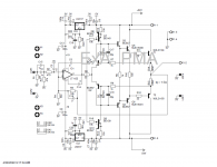
Below is the circuit schematics, THD vs. power plots at 1kHz and 5kHz and the 1kHz spectrum. Output noise is 23uV over 20Hz-22kHz unweighted. This was measured with OPA637 at the place of IC1.


The amp uses modified output stage from ExtremA by Sander Sassen which was put in the loop of a good opamp. The output stage uses local NFB and has vanishingly low distortion below 0.001% itself, but quite high output impedance of 0.235 ohm. In the opamp feedback loop the distortion falls below 0.0001% and the output impedance becomes negligible.
Below is the circuit schematics, THD vs. power plots at 1kHz and 5kHz and the 1kHz spectrum. Output noise is 23uV over 20Hz-22kHz unweighted. This was measured with OPA637 at the place of IC1.

I did not think about it, however the output stage has 12 discrete transistors, so is it a chipamp? I would never have expected a question like this.Should this not belong to the chipamp category ?
Regards,
Patrick
Is LM4702 with discrete output stage not a chipamp then ?
Unless of course you replace the DIP8 opamp with a discrete one. 😉
Patrick
Unless of course you replace the DIP8 opamp with a discrete one. 😉
Patrick
Chip Amps as far as the forum are concerned normally relate to complete amps on a monolithic or hybrid chip such as TDA2030/LM3886/TBA820 etc or the hybrid STK variants.
The one in this thread would be classed as a discrete amp and so solid state is the proper place.
The one in this thread would be classed as a discrete amp and so solid state is the proper place.
LM4702 is a power amplifier, OPA637 or LT1122 used here as an input stage are low power opamps. The key here is in the output stage and the output stage is discrete. What is your point? Any problem? I do not understand you, Patrick.
Quad 405 is a common power amp, opamp front end and 10 bjt transistors. We would never refer to that as a chip amp.
You can refer to the original ExtremA here :
https://www.diyaudio.com/community/threads/extrema-class-a-strikes-back.96853/post-1142320
Patrick
https://www.diyaudio.com/community/threads/extrema-class-a-strikes-back.96853/post-1142320
Patrick
Yes. I need to prepare it with some comments.Would you give schematic with values of components .. transistors number ....
Thank you 😉. It is extremely impractical making a lot of heat. It was rather a concept to check what we "can" do.Very nice! ASR would go bananas ;-)
I would like a pair....
//
Well up to some limit, I need to re-measure it. Of course output L//R would make it unconditionally stable.How does it perform with reactive (capacitive) load ?
Patrick
Some step/square responses below.


I remember vaguely reading a report from you some years ago, showing the step responese of a power amp with 1µF at the output.
I wonder if you have a "standard" stability test, and if yes, whether you would kindly share.
Thx,
Patrick
I wonder if you have a "standard" stability test, and if yes, whether you would kindly share.
Thx,
Patrick
1.There are 4 more BE junctions to compensate...q1 can't deal with q3xq5 runaway currents.Sassen does it and you can't really escape it especially with a class A hot amp.You might really need to compute the d1,d2 zenner tempco into this or just put two diodes in series with q1, q2 collector.Relying on the op-amp's offset to make the tempco...
Unfortunately this topogy's performance is really sensitive to the idle current, its performance dropping a lot within class AB realm.I didn't know it's Sassen design when i made my bootstraped version, but I know why I opted for modifying it for class B operation where you can actually get better results than class A due to the unique possibility to use the output trz junction to bias the input pair of transistors very similarly to Blomley or Hartsuiker design.Other than that it makes for a pretty simple and viable class A design.
Unfortunately this topogy's performance is really sensitive to the idle current, its performance dropping a lot within class AB realm.I didn't know it's Sassen design when i made my bootstraped version, but I know why I opted for modifying it for class B operation where you can actually get better results than class A due to the unique possibility to use the output trz junction to bias the input pair of transistors very similarly to Blomley or Hartsuiker design.Other than that it makes for a pretty simple and viable class A design.
Attachments
Last edited:
Would you give schematic with values of components .. transistors number ....
This is the complete schematics with part numbers. IC1 supply voltage is to be adjusted by R22/R23 and R20/R21 between 18-20V, according to the opamp used. LT1122 tolerates up to +/-20V according to the datasheet. OPA637 max. supply is +/-18V. I run it at +/-19V, which exceeds parameters specs, but it works so far.
Idle current is 1.5A and is measured as a voltage across R14 and R15. Voltage across emitter resistors is used for a local NFB via Q1 and Q2.
C19 and C20 reduce HF distortion and improve HF linearity considerably by reducing rail modulation by input signal.
To achieve large S/N at mains frequency and multiples great care must be taken in signal GND track routing. Small signal GND to be routed separately and connected with large current GND at the point LSP7 where PSU 0V terminal is soldered into PCB. The difference in mains residual can be as large as 30-40dB if the small signal GND is routed improperly. This and rail modulation by input signal is difficult to see from simulation only.
Idle power dissipation is about 75W per channel. An appropriate heatsink with low thermal resistance must be used. The one shown in my sample photo is insufficient for normal operation. I was using 19" 3U case with side heatsinks with fins and low thermal resistance during the normal listening operation of the amp.
Attachments
Too hot to be practical 😀.
I am owing distortion plot into 4ohm load. So here it is, still very low distortion. At about 18W it moves to class AB and keeps low distortion up to some 22W, but immediately after transition we can see higher order distortion components that have been only H2 and H3 in class A.

And THD vs. frequency

I am owing distortion plot into 4ohm load. So here it is, still very low distortion. At about 18W it moves to class AB and keeps low distortion up to some 22W, but immediately after transition we can see higher order distortion components that have been only H2 and H3 in class A.
And THD vs. frequency
Last edited:
- Home
- Amplifiers
- Solid State
- Small class A amplifier with THD below 0.0001%