I wonder if you are detecting the change in distortion as the bias requirement for minimum distortion changes with temperature?
What happens if you increase the output bias slightly and test again with the output bias reduced slightly. Maybe +-10% from your present bias value.
Changing the bias does absolutely nothing. Either driving a load, or not, under biasing or significantly over biasing, the distortion performance is being swamped by something else.
Would changing the driver emitter resistor show a change in distortion?
This is a CFP output stage and has no driver emitter resistors, like an EF. Would you be referring to the resistors that connect from the driver collectors to the supply rails?
Last edited:
The open loop gain of the amplifier should increase with temperature, as the current gain of *all* transistors increases 🙂
Am I right in saying that if this was going to affect anything it would only do so at high frequencies?
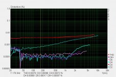
I tried measuring the VAS output on its own and got the attached image.
Measuring the input stage would be a tad harder I presume as it's got a current output.
I'm not entirely sure how useful this is as the 2nd harmonic is clearly not showing what goes on at the output. Also this was done with zero load on the output, whenever the output was loaded the distortion fell to pieces.
Either way it shows the same flat line 3rd harmonic. I assume this shows that the problem is located either in the VAS or input stage.
Attachments
I tried adding in a VAS buffer, the type that uses a shared CCS with PNP transistor.
This simulated very well and lowered THD nicely, however in practise it did nothing 😛 Still the same 3rd order.
I also tried messing up the input stage by severely limiting the current. This successfully(I think) showed what a borked input stage looks like. Both 2nd and 3rd order rising steeply as frequency increases.
At least the input stage is getting enough current to drive the rest of the amp. If the input pair were poorly matched I'd see problems with 2nd harmonic, which I don't. If the driving capability of the input stage was under question then the 3rd order should get worse as frequency rises, this is not the case.
If the VAS were to blame for the high 3rd order I'd expect buffering it to do at least something.
Changing components in the input stage, from low beta to high beta devices, does nothing to alter distortion, neither did running it in inverting.
Completely altering the VAS transistors does nothing at all to alter the distortion.
In the second PCB I tried the split 47r into 11r/33r etc thingy on the VAS, this did nothing.
I've tried a polyprop film cap on the input, again this did nothing.
I've tried running the amplifier with single pole compensation, this did nothing. I've tried replacing the compensation caps with a few different caps, this did nothing.
Removal of the small cap at the start of the feedback take off point did nothing.
I've tried several different feedback take off points, this does nothing.
Distortion 1: Input stage distortion. I don't appear to be suffering from this.
Distortion 2: VAS distortion, should be 2nd order if it's present and should also rise @ 6dB/octave as P1 is reached. I might be suffering from this on top of output stage distortion, a 12dB increase in 2nd harmonic is present and is shown in post 73.
Distortion 3: Output Stage distortion. This is to be expected.
Distortion 4: VAS loading. If present should show some changes as P1 is reached as the linearisation effect of feedback changes. Also the loading of the VAS changes with respect to load placed on the amplifier and this doesn't alter the performance I'm getting.
Distortion 5 and 6 are related to half wave sine pulses interfering in some way with the rest of the amplifier. Are not present in Class A and are also affected by the driven load. I do not experience either of these, unless their contribution is entirely 3rd harmonic at higher levels, in which case it's being completely swamped by something else.
Distortion 7: NFB take off point. I've experimented with this to no effect.
Distortion 8: Capacitor distortion. I've tried different caps in the compensation, in the input stage, in the feedback network, in the zobel, nothing changes.
DIstortion 9: Magnetic distortion. No change in distortion performance came about by connecting the amplifier through the output relays.
Distortion 10: Input current distortion. Comes about when the amplifier is driven by an appreciably high source impedance. Not a problem here, in fact I tried lowering the output impedance of the pre amp and it did nothing.
Distortion 11: Premature Overload Protection. I've disabled the SOAR protection and this did nothing. I've also altered the protection on the VAS and this also does nothing.
What the heck am I supposed to make of all of this? I know this can't rule out everything. I tried driving the amplifier with another low distortion source that also yielded the same results. The only sources that showed any kind of improvement had 0.003-4% distortion when measured individually. And when driving the amplifier this dropped down to 0.002% or so, but that can easily be attributed to the harmonics produced by the amplifier cancelling the harmonics produced by the two laptops, which is what they were.
The only thing I can think is that there is perhaps one track on the PCB that's inducing something, but figuring out which one it is is anyone's best guess.
I can build another version with a cascode input stage. I could also build another version with a cascoded and buffered VAS. But then that's a completely different design and shouldn't be necessary if Self is to be believed.
Instead of trying to fix the problem are there any things that I can do to the amplifier design that would highlight what area could be causing the problem? Instead of making it better, make it worse?
If any of you are as confused as I am, please say so 😀 Or alternatively if you have a hunch at what could be the problem, if it's feasible to try it, I'll give it go. Do any of you think that I am expecting too much? In that you'd be happy if the amplifier performed as it's doing now? And if you were not happy, what would you be doing in my shoes to try and solve the problem?
I am getting close to just giving up and building another 8 channels as they are. After all I can get 10 watts @ 8 ohms, out of these before the third harmonic problem. And 99% of the time no one will use more then that. But it would be nice to track down where the problem is.
Many thanks for even reading all of this as it is quite a lot and many more thanks for any assistance/ideas no matter how crazy.
Last edited:
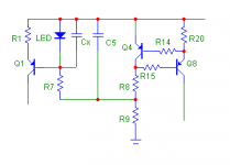
Most sensitive point to induction is conection between colector of Q9 to base of Q5. It should be as short as possible and do not cross any track (component) feeding current. It is fed under C7 and R13, it seems to me as not good solution .To get "blameless" performance is very layout critical . I had the same experience, changing the placing of one resistor about 10mm and 90deg. rotation changed distortion performance from 0,02% under 0,001%.. You tried to remove Q17 ?
But You wrote, distortion apears abrupt, at same level, so it is voltage dependent, something like partially breakdown in some component exposed to voltage swing?
But You wrote, distortion apears abrupt, at same level, so it is voltage dependent, something like partially breakdown in some component exposed to voltage swing?
Most sensitive point to induction is conection between colector of Q9 to base of Q5. It should be as short as possible and do not cross any track (component) feeding current. It is fed under C7 and R13, it seems to me as not good solution.
Thank you for your response.
It also feeds under R6, although the current through that resistor should be very small and constant.
It should be fairly easy to redesign the board to try this out. I'm thinking of relocating C7 and D1 and moving the VAS closer to the input stage.
Any current flowing through R13 should vary with frequency though right? As it's part of the 2pole comp circuit? I have tried the amp 1 pole, with the removal of R13 and this didn't change the 3rd problem.
To get "blameless" performance is very layout critical . I had the same experience, changing the placing of one resistor about 10mm and 90deg. rotation changed distortion performance from 0,02% under 0,001%.
Hehe the trouble is finding out which one.
You tried to remove Q17 ?
Yes, no effect.
But You wrote, distortion appears abrupt, at same level, so it is voltage dependent, something like partially breakdown in some component exposed to voltage swing?
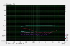
Yeah this is the confusing part. Whether the amp is driving the sound card alone, or a load the 3rd order remains roughly unchanged.
At 30 volts p-p is when the 3rd order starts to dominate. Driving the sound card, distortion is low...

If you then attach a 9,4 ohm load the distortion increases by a small amount, but this is as expected...

Then once again it increases as I drive the 4.7 ohm load, but that's to be expected also...

The absolute magnitude of the 3rd order at low frequencies actually decreases a little as the output current goes up.
If I drop the drive level down to 20v p-p the third order blends in with the 2nd @ 0.0003-5%, until around 5khz.
No load...

Driving 9.4 ohm, showing increased distortion from the output stage.

As of now the output current doesn't affect the third order much at all. It seems, just like you said...
Something like partially breakdown in some component exposed to voltage swing?
This could be a tiny induction from somewhere. But where? I can pass the wire carrying the output of the amplifier, whilst it's driving a load, all over the different sections of the PCB and it does almost nothing.
Everything keeps leading back to nothing, which I guess is possible. This is a measurement artefact of some sort, but I find that hard to believe. Both the amplifier and sound card have the same input impedance 10k. If I remove the amplifier from the signal chain the third harmonic vanishes. I've tried inserting another amplifier of similar design ( Quad77 integrated, its a CFP amp of similar output power.) in place of the one I've built and it doesn't show the same third harmonic problem. The Quad actually performs very well, although it's high frequency distortion isn't as low as the one I've built.
Perhaps nonlinear cb capacitance of Q8, try to place capacitor (47uF?) between base Q8 and Vcc bus..Or cascoding current source for VAS.
Hi,
would the performance improve if Q8 was changed to become the complement to Q6.
I dislike Self's use of the CCS control voltage (Q8,Q4) to also set an uncontrolled voltage for Q3. If Q4 is actively reacting to Q8's needs then that variation is needlessly being fed to Q3 as well. Although I dislike it I have no evidence to show it cannot work. Reading of Self's slew rate asymmetry and the steps he took to improve slew rate seem to show he did not understand the full workings of this dual CCS.
Sure, it is much better to use two independent CCS for input and VAS. And replacing R15 with short (jumper) can also help.
Attachments
Last edited:
I've read here that the coupled CCS for LTP and VAS has a protection/shutdown effect when driven into overload.
Is this paramount and can this protection be provided in a better sound quality way, if the two stages have separate CCS?
D1 should never have an AC voltage across it when the amp is operating within it's specification. The DC voltage is ~output offset voltage.
Is this paramount and can this protection be provided in a better sound quality way, if the two stages have separate CCS?
D1 should never have an AC voltage across it when the amp is operating within it's specification. The DC voltage is ~output offset voltage.
Last edited:
Perhaps nonlinear cb capacitance of Q8, try to place capacitor (47uF?) between base Q8 and Vcc bus..Or cascoding current source for VAS.
This was interesting. And not just because the performance literally turned to cow dung. But more for what it ended up doing to the third harmonic. My guess is that this is just some form of cancellation from somewhere. But I don't fully agree with the results based simply on that.
All of the other harmonics increased as a result of adding in that cap, but they do not vary much with frequency. You'd figure that adding the cap would result in a net increase of 3rd harmonic too.
The old third harmonic problem doesn't vary much with frequency. If adding in the cap would have produced another source that remained flat with frequency, then surely the net result should be a flat increase (if constructive), or decrease (if destructive) or the overall distortion performance.
Now induction distortion changes with frequency, but if adding in the cap caused this to happen, surely all the harmonics would change as a result, rather then just one.
Either way the level of third harmonic from 800hz onwards does what I'd expect it to do if the amp was behaving properly in the first place.
Attachments
I dislike Self's use of the CCS control voltage (Q8,Q4) to also set an uncontrolled voltage for Q3.
Sure, it is much better to use two independent CCS for input and VAS. And replacing R15 with short (jumper) can also help.
I can easily add in another transistor and create two separate current sources. One thing Slone does well (at least according to me) is his descriptions of various constant current designs.
I've read here that the coupled CCS for LTP and VAS has a protection/shutdown effect when driven into overload.
Is this paramount and can this protection be provided in a better sound quality way, if the two stages have separate CCS?
I never intend driving the amplifiers into overload, except in testing. Or are you implying that due to a failure in another stage it could cause the CCS to go out of control and this version is self limiting so wont blow up 😛
D1 should never have an AC voltage across it when the amp is operating within it's specification. The DC voltage is ~output offset voltage.
Have you checked the effects of D1 in the feedback circuit to the distortion performance?
I thought D1 was present to prevent the rail voltage from being thrown at C5 in the event of a some sort of failure. I did try disconnecting D1 a few days ago, just to see if it was doing anything and indeed it was not.
Currently I'm looking at two separate constant current sources along with a few PCB changes that put the VAS closer to the input stage.
Perhaps nonlinear cb capacitance of Q8, try to place capacitor (47uF?) between base Q8 and Vcc bus..Or cascoding current source for VAS.
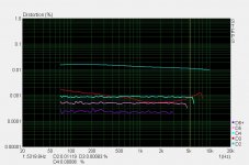
I tried this again with different sized caps.
The first attachment is with a 22u the second is with a 220u.
I don't exactly know what's going on here but the larger the cap is made the better the third harmonic becomes, even though everything else is significantly worse.
Also when a load is placed on the amp all the distortion products rise.
Attachments

replace the electrolytic with a 1uF or 2u2F film cap.
test distortion again.
I expect the LF end to be much worse, but what about the Mid and HF end?
Then add a 470uF to the film to change the LF end.
test distortion again.
I expect the LF end to be much worse, but what about the Mid and HF end?
Then add a 470uF to the film to change the LF end.
replace the electrolytic with a 1uF or 2u2F film cap.
test distortion again.
I expect the LF end to be much worse, but what about the Mid and HF end?
Then add a 470uF to the film to change the LF end.
Maybe you've misunderstood what's going on here. The high frequency response is improved by increasing the capacitor value (for third order), decreasing it improves low frequency performance.
Using just a 1.5uf film cap yields no real effect on the third harmonic at high frequencies, because it is not big enough.
If you look at the response with the 22uf lytic you can see that it's almost as if a high pass has been placed on the distortion. Decreasing this down to a 1.5uf causes the corner frequency to increase, but as the cap isn't large enough it has almost zero effect on the third order and this is at all frequencies.
I've already got another board etched, I just need to drill it before stuffing it with components. Watch this space.
that's not what I see.
Above 1kHz, it appears that all harmonics are lower with the 22uF, except the 3rd.
Below 1kHz, it appears that all the harmonics are lower with the 22uF, again except the 3rd, but in this lower frequency region the 3rd is much worse.
Is your sampling rate 44ks/s?
That makes the maximum frequency ~21kHz to 22kHz. The highest frequency for which you can get reliable distortion results will be ~ 2150Hz with that sampling rate.
that's not what I see.
Above 1kHz, it appears that all harmonics are lower with the 22uF, except the 3rd.
Below 1kHz, it appears that all the harmonics are lower with the 22uF, again except the 3rd, but in this lower frequency region the 3rd is much worse.
Please bare in mind that the scale is different for some of those graphs. Some of them have 1% as the max some have 100%. I apologise for the mix up but sometimes I forget to put it from 100 to 1%.
There are some minor changes at high frequency with regards to cap size, but not a lot.
Is your sampling rate 44ks/s?
That makes the maximum frequency ~21kHz to 22kHz. The highest frequency for which you can get reliable distortion results will be ~ 2150Hz with that sampling rate.
The sampling frequency is 48khz. Why does it limit you to 2150Hz or similar? 24khz being the Nyquist frequency. A 12khz fundamental would produce a 24khz 2nd harmonic, which should be perfectly rendered by the ADC and hence the level of the harmonic determinable. The highest frequency you could get 3rd harmonic for would be an 8khz fundamental, which is what the program would seem to indicate also. Obviously I'd expect the absolute performance at extreme high frequencies to be somewhat haphazard, but the results seem fairly repeatable and correlate well with predicted theory, except for the 3rd harmonic.
I have built another channel, moving the VAS closer to the input stage and moving components away from bridging the trace from the input stage > VAS.
I have also added in separate CCs for both the input stage and the VAS.
No change, pretty much the same end result. The absolute performance varies by a smidgen, but the overall trends are exactly the same. 2nd harmonic if anything is slightly worse. But still within 0.000x%.
I have also added in separate CCs for both the input stage and the VAS.
No change, pretty much the same end result. The absolute performance varies by a smidgen, but the overall trends are exactly the same. 2nd harmonic if anything is slightly worse. But still within 0.000x%.
I am going to end up making 10 of these and I have a lot of raw PCB material and a ton of chemicals. On top of this I also have a decent amount of time on my hands.
The performance the amplifiers are providing now, for all intents and purposes is acceptable. I have no real issue with building 10 of them. As stated before 99.9% of the time they'll be using 1-5 watts maximum. And even then 0.004% THD @ full power is nothing to shake a stick at.
If any of you have any radical suggestions towards the PCB I really don't mind trying them out. I would like to keep the overall form factor the same, the size and shape is important. But beyond that I'll give anything a go - as long as the performance is not significantly worse then what I'm currently getting, it will be usable.
I am of course assuming that the circuit is capable of delivering the performance I am expecting it to provide.
My own simulations back up the fact that I should.
On top of this Self has built many amplifiers and measured them also - his own driving goal along the way being, to arrive at 'blameless' performance. And when he doesn't end up with it, he wants to find out why. Those circuits that he has built, he claims, are very similar, if not identical, to some of the schematics illustrated throughout his book. So if they didn't work I'd be surprised.
If the circuit itself is capable, then that leaves three areas for error.
1) The PCB.
2) The components.
3) There's another source of distortion not intrinsic to the amplifier and it appears as a result of the measurement system.
The only thing left of the components are the pre drivers. Everything else has been prodded, poked or changed for something else. If those components are to blame I'd be surprised.
I have also faffed about with the test system, altering grounding within the equipment, changing some components, fiddling about with gain settings and testing other pieces of equipment. All of this points towards the measurement system being capable.
That leaves the PCB.
Throw any ideas at me. If they are not going to do any outright harm, I'll give them a go. For example I could take all the power traces to the copper bottom, bringing it up through vias to where it's needed, etc. I can't see why this would do anything, but I can also see that it shouldn't really make things any worse.
- Status
- Not open for further replies.
- Home
- Amplifiers
- Solid State
- Slones 11.4 'Blameless'