As the distortion is largely unaffected by the load placed on the amplifier. I think it's safe to say, that currently, the distortion is being dominated by something other then any possible injection from the supply rails, or contamination of the signal ground.
The input stage is by and large quite isolated. It's kept very compact by the use of surface mount components and it has the pre driver heat sinks acting as a shield, between it and the output stage.
The other path that could otherwise lead to a problem is maybe the feedback connection. Referring to the PCB layout, R10 and C6, they both have a trace running directly beneath them. This trace has the output voltage running through it. Also R17, this has the output voltage running directly though it too and it bridges over the feedback trace.
Would it be worth trying another board design where I reroute those things away from the feedback trace?
C6 isn't the cause of the distortion itself. C9 and C10 (2pole comp) are NPO/COG but could possibly be a problem, but there's no way to tell without trying different components here.
Edit - I tried replacing R17 with a through hole and it made no difference what so ever. The resistor was soldered in place from two points a distance away from teh feedback track, so I doubt it's that.
Last edited:
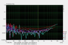
This for example is the distortion with the amp driving a 9.4 ohm load @ 28 volts p-p.
When driving a 4.7 ohm load it looks virtually identical, except that the 2nd order by 10khz is @ 0.004% rather then 0.002% as with the 9.4 ohm load. This is entirely expected. Also the performance is virtually 'blameless' and I couldn't ask for anything more.
The problems occur beyond this point. Something somewhere causes 3rd order to shoot up (2nd order goes up too but it isn't so pronounced), irrespective of the current draw placed on the amplifier.
I tried increasing the current through the input stage by a little, this did nothing, so that's not the cause.
I have ordered some different capacitors for the 2pole compensation caps, just to see if they make any difference at all.
If not, I'm thinking that there's a problem with the feedback take off point. And if no one responds with anything I'm just going to go ahead and try another board design, whilst tidying up the 'output' section of the amplifier a bit.
Edit - try attaching the picture -.-
Attachments
with TPC resistor conected to GND..
I tried that it made things worse by a tiny bit.
Have you tried cascodes in the VAS transistors?
Non-linear capacitances and hFE changes with Vce are a 3rd harmonic distortion source too, and it's not load dependent at all.
Input stage may benefit too if the amplifier is non-inverting (LTP transistors are subject to signal dependent Vce even with no rail sag).
Non-linear capacitances and hFE changes with Vce are a 3rd harmonic distortion source too, and it's not load dependent at all.
Input stage may benefit too if the amplifier is non-inverting (LTP transistors are subject to signal dependent Vce even with no rail sag).
Have you tried cascodes in the VAS transistors?
Is that needed here? Self says, that using an emitter-follower VAS stage is another way to reduce distortion 4 (VAS loading distortion) and that is what this amplifier is using right? He also uses the emitter-follower type in almost all the designs in his book.
He does use the MPSA06 transistor instead of the 2SD669 that Slone likes to use. Whether or not this would make a large difference I don't know. The MPSA does have a higher minimum hFE from what I can see and I do have some of those arriving tomorrow. So I could try those instead and see if anything changes.
Input stage may benefit too if the amplifier is non-inverting (LTP transistors are subject to signal dependent Vce even with no rail sag).
The amplifier is non inverting, but once again I would be surprised if there was something wrong with the inherent design. The same topology is used over and over again in lowish powered designs throughout Self's books. The only thing different is the transistors used and different CCS values etc.
I'm more inclined to believe that perhaps the transistors are at fault perhaps. Self states that having transistors on the input pair with a high hFE is beneficial. The 5401s that I'm using aren't all that great in that respect. I wanted to try the 2sa1587 but I can't find anywhere as of yet, to buy them from.
Another thing that perhaps hints at the input stage being at fault is the high DC offset. I'm getting 70mV which to me is bit too high and unusual - All the other amplifiers I've built, to the same design, but with Slone's poor PCB, had DC offset usually below 5mV and always below 10. Those used entirely through hole.
I have tried changing one of the input pair to another 5401 but that made it worse, the transistors are all from the same reel. I've also observed the DC offset as I've put my finger on top of the 5401s, causing the temperature to change and the drift is always very small, +- 10mV.
You are dealing with very low levels of distortion, where details matter a lot.
Yes I appreciate that, are you referring to the use of cascoding the various stages?
Or to the fact that getting the right transistor combos and surrounding component values is essential too? (Obviously it's essential, but I mean if I get those right the design should essentially work as proposed.)
I think the overall design, ie what type of components (and by this I mean resistor/capacitor) are used and where they are placed is solid enough. This type of design is used throughout Self's book and if it was inherently incapable of the performance, that he pretty much bases his book on, I would be very surprised.
I am of course entirely open to the fact that using the right transistors for the job is absolutely necessary and also of the fact that these need to be used in the correct way. Slone has done nothing but let me down with regards to the absolutes with the designs he's published. Either not working properly, or grossly missing their stated specifications. So I wouldn't be surprised at all, if once again, his design misses the mark, either by incorrectly used components or simply using the wrong type.
With regards to the board layout.
1) As the distortion doesn't change, or isn't made worse by changing the driven load. I think this shows that half wave sine pulses are not contaminating the end results. Or at least they are not the dominating factor at this point. Am I correct in assuming this?
2) Self states that an incorrectly placed feedback take off point is a non issue in class A amplifiers. This is (I am assuming) because a constant amount of current is already flowing through the output devices. There are no rapidly changing current demands between the two rails and no turbulent summation at the output between the RE resistors. And as a result this makes it impossible to contaminate the feedback in a Class A amp.
If this is correct, then surely I am not experiencing the effects generated by an incorrectly placed feedback loop. If I were, then surely changing the current demands placed on the amplifier would affect the distortion in some way.
And if that is the case then surely an amplifier driving infinity, wouldn't show signs of an incorrectly placed feedback loop. Because if it's driving infinity (it's actually driving the sound card + scope which is a very benign load, but it's a load at least), surely the quiescent current would put the amplifier into class A.?
I am trying to determine if the PCB layout is at fault. I don't want to go altering the design (adding cascodes) and buying several different types of transistor simply on a hope that it will correct the problem.
So far no one has mentioned if the PCB layout looks adequate. From the results I've measured I am driven to believe that it is. For if it were not I would expect to get something different.
Clearly I don't have a huge amount of experience in dealing with things like this. But from what I've understood from Self's book, I am not dealing with a grossly miss designed PCB. But then again, as you said, Eva, with distortion levels this low all the tiny details matter, it's just a case of trying to find out what they are.
Try making the amplifier inverting to make input transistors work at constant Vce, minimum PCB changes should be required.
That way you will be removing the errors due to Vbe, hFE (Early effect) and capacitance modulation by a varying Vce. These errors apply directly to the error voltage sensed by the input LTP and thus no amount of NFB can help, as the wrong error voltage is being sensed.
That way you will be removing the errors due to Vbe, hFE (Early effect) and capacitance modulation by a varying Vce. These errors apply directly to the error voltage sensed by the input LTP and thus no amount of NFB can help, as the wrong error voltage is being sensed.
Try making the amplifier inverting to make input transistors work at constant Vce, minimum PCB changes should be required.
That way you will be removing the errors due to Vbe, hFE (Early effect) and capacitance modulation by a varying Vce. These errors apply directly to the error voltage sensed by the input LTP and thus no amount of NFB can help, as the wrong error voltage is being sensed.
I'll first have to figure out how to do that.😀
Can't I just tie the non inverting input to ground and then treat this like an opamp?
Presumably I want to keep the input impedance the same to satisfy other criteria of the amplifier.
Do I need to do anything specific with the feedback, or can I just leave it as it is. Tying the non inverting input to ground, connecting the signal input through a 10k resistor to the inverting input, then connecting the feedback to the inverting input via another 10k?
Hi,
are you using the 2sd669 as a VAS?
What is driving it?
I think the input pair give rise to 2nd harmonic, if not well matched and your output offset seems to indicate this might be the case.
What are the currents in the mirror resistors and in the degeneration resistors?
are you using the 2sd669 as a VAS?
What is driving it?
I think the input pair give rise to 2nd harmonic, if not well matched and your output offset seems to indicate this might be the case.
What are the currents in the mirror resistors and in the degeneration resistors?
Last edited:
With 150/330 pf we're at about 10 degrees by the time 100khz is reached. If that's what you were asking.
I'm not entirely sure how to simulate the unity loop gain. Are you asking for the open loop gain?
Hi,
Please take some time and read about negative feedback. It was written about it numerous times on this forum. Also, google is your friend. If you are using LTSpice then I suggest you to look up the file LoopGain2.asc in Examples directory and see how to simulate loop gain. I expressed concerns that 150pF capacitor could set ULG frequency too low. It's a good start to put ULG frequency around 1+ MHz.
Also, distortion doesn't come from only one mechanism, it comes from many mechanisms working concurrently. Maybe, you should apply more then one advice given in this thread to achieve lower distortion.
P.S. I don't like the choice of Q5. High beta, low Cob should be chosen here.
Cheers,
Nesa
10 cents
hello
Re post 40.my(thick) head say's star earths need star power(tracks) at least to the nearest decoupling farads.
regards
Max
ps no nodal inrerractionwise
hello
Re post 40.my(thick) head say's star earths need star power(tracks) at least to the nearest decoupling farads.
regards
Max
ps no nodal inrerractionwise
Last edited:
the ratio of R20:R22 is too close to unity.
The VAS is set up to pass ~6mA.
The protection transistor is starting to limit at 8.5mA.
I reckon on a ratio of 3:1.
Split the 47r into 13r+33r and take the junction to the protection resistor.
with 47r the swing in the VAS is only +-2.5mA (on symmetrical signals). Through a two stage output there may be insufficient current to the load before the VAS starts hitting it's current limit.
Last edited:
Can't I just tie the non inverting input to ground and then treat this like an opamp?
Presumably I want to keep the input impedance the same to satisfy other criteria of the amplifier.
Do I need to do anything specific with the feedback, or can I just leave it as it is. Tying the non inverting input to ground, connecting the signal input through a 10k resistor to the inverting input, then connecting the feedback to the inverting input via another 10k?
It's mostly like an op-amp, for example you can inject the inverting signal to the inverting input through the negative lead of C7 and by grounding the non-inverting input. That would be a low impedance input, though.
Last edited:
Alrighty I'm back, the internet died for a day. Openreach are installing FTTC in our area so the internet's been going up and down the last week. Normally they turn it back on at the end of the working day, but not yesterday, lucky us. I'll be interested to see how the internet performance changes with this though.
Lots of replies to respond to.😀
Mmm I tried simulating using the inverting input. The amplifier there wasn't so happy if I tried altering things to create a more friendly input impedance. Luckily for me though the preamp is more then capable of driving low impedance, so I tried this.
The distortion behaves in exactly the same way and the DC offset shoots up to 210mV.
Lots of replies to respond to.😀
It's mostly like an op-amp, for example you can inject the inverting signal to the inverting input through the negative lead of C7 and by grounding the non-inverting input. That would be a low impedance input, though.
Mmm I tried simulating using the inverting input. The amplifier there wasn't so happy if I tried altering things to create a more friendly input impedance. Luckily for me though the preamp is more then capable of driving low impedance, so I tried this.
The distortion behaves in exactly the same way and the DC offset shoots up to 210mV.
I think the input pair give rise to 2nd harmonic, if not well matched and your output offset seems to indicate this might be the case.
What are the currents in the mirror resistors and in the degeneration resistors?
Yes this is exactly what Self says. In simulation I tried miss aligning the input pair by altering the value of of one of the degeneration resistors. The result? Increased 2nd order that kept getting worse the more the drive level was increased.
Signs of this are apparent in the real life amplifier.
With regards to the offset.
The two degeneration resistors . R2 and R3. These have 206 and 209mV dropped across them. This shouldn't cause that much offset according to Self.
He states a larger cause of offset is beta mismatch causing a differing amount of current to flow through the input resistor R4 and the feedback resistor R10.
I can measure the voltage drop across R10 at about 200mV however the drop across R4 is more like 150mV. So clearly the input transistors can't be matched very well.
I had wanted to try out 2SA1587 on the input stage. These appear to be the surface mount versions of the 2SA970s Self makes mention of in his book. And then to also try the 2SC4117s in the current mirrors. These are high beta devices and from everything he says should be better suited to the job. The only problem is I haven't been able to find anywhere to buy them from.
I can always try the MPSA06/56s he makes heavy use of.
Hi,
are you using the 2sd669 as a VAS?
What is driving it?
Yes 2sd669 in the VAS with another 669 driving it.
I've tried changing the VAS transistor to an MPSA06 and this altered absolutely nothing.
I have also tried increasing the VAS current to 9mA and this made no change either.
Hi,
change the VAS to a 5W to 10W, medium hFE, low Cob, 100mA to 200mA transistor.
Change the VAS EF to a 400mW to 625mW, high hFE, low Cob, 50mA to 100mA transistor.
change the VAS to a 5W to 10W, medium hFE, low Cob, 100mA to 200mA transistor.
Change the VAS EF to a 400mW to 625mW, high hFE, low Cob, 50mA to 100mA transistor.
the ratio of R20:R22 is too close to unity.
The VAS is set up to pass ~6mA.
The protection transistor is starting to limit at 8.5mA.
I reckon on a ratio of 3:1.
Split the 47r into 13r+33r and take the junction to the protection resistor.
with 47r the swing in the VAS is only +-2.5mA (on symmetrical signals). Through a two stage output there may be insufficient current to the load before the VAS starts hitting it's current limit.
I have tried lowering the value from 47r to less and this didn't change anything. I've also tried testing the amp without the protection transistor in place and this didn't change anything either.
- Status
- Not open for further replies.
- Home
- Amplifiers
- Solid State
- Slones 11.4 'Blameless'