I altered one of the input transistors and now I'm getting ~5mV offset, which is much more satisfactory. This didn't change the distortion though, so the extra 2nd order that I am seeing isn't a result of the mismatch.
I have tried different caps in the 2pole compensation and this changed nothing too.
I have tried different caps in the 2pole compensation and this changed nothing too.
simply changing the 47r changes the degeneration of the VAS and thus changes the amp's behaviour.
Split the resistor once you are happy with the final components values and PCB layout.
If the VAS was being prematurely limited, a temporary check for this would be the removal of Q17 right?
Hi,
Please take some time and read about negative feedback. It was written about it numerous times on this forum. Also, google is your friend. If you are using LTSpice then I suggest you to look up the file LoopGain2.asc in Examples directory and see how to simulate loop gain. I expressed concerns that 150pF capacitor could set ULG frequency too low. It's a good start to put ULG frequency around 1+ MHz.
Also, distortion doesn't come from only one mechanism, it comes from many mechanisms working concurrently. Maybe, you should apply more then one advice given in this thread to achieve lower distortion.
P.S. I don't like the choice of Q5. High beta, low Cob should be chosen here.
Cheers,
Nesa
I am aware of negative feedback and what it's there for and what it does. However I thought incorrectly applied feedback would cause stability issues. I am seeing none of that here, except...
I do get an amount of sticking on the negative rail when the amp clips. If Q17 isn't present on clipping the negative rail clipping does something really ugly and R22 has a lot of current thrown through it.
It's hard to describe really ugly and I don't want to force the amp to reproduce it just so I can grab a pic on the scope.
It kinda looks like the attached pic. Where the negative portion should simply be a flattening of the sine wave against the negative rail, it appears to reflect itself off the rail as if it were a mirror. I cannot remember if anything is actually 'flattened' against the rail, or if it's entirely reflected back.
This only happens if Q17 isn't in place and with it there I get rail sticking. I can force it to show signs of instability, but I really need to make the amp clip badly for this to happen, we're talking 10-20% THD.
The higher in frequency I go the worse this sticking appears to be.
This is all with no load attached and 125mA resistors in the fuse sockets. I don't really want to push the amp into doing this with a load attached.
I can show a picture of mild clipping, on the scope at 10khz if you want as that highlights what's going on very well.
Attachments

KSC1845/KSA992 for the VAS EF?
The surface mount versions of those look nice for the input stage too.
Looks okay for the VAS tranny.
Those look quite similar to the 669. Is there anything wrong with the 669 for the VAS transistor?
There's this that has lower Cob.
The surface mount versions of those look nice for the input stage too.
Looks okay for the VAS tranny.
Those look quite similar to the 669. Is there anything wrong with the 669 for the VAS transistor?
There's this that has lower Cob.
Hi,
the E version of the 50mA and 100mA transistors will do the VAS EF and the VAS. Anything similar would do here.
The 669 and similare 1.2A devices are good for output drivers, not VAS.
the E version of the 50mA and 100mA transistors will do the VAS EF and the VAS. Anything similar would do here.
The 669 and similare 1.2A devices are good for output drivers, not VAS.
removing the VAS protection can destroy Q5.
There were a couple of threads in the last year that discussed this in detail.
They solved it by omitting the protection and adding a Q5 collector resistor to ground. This limited EF current to a safe level during overload.
There were a couple of threads in the last year that discussed this in detail.
They solved it by omitting the protection and adding a Q5 collector resistor to ground. This limited EF current to a safe level during overload.
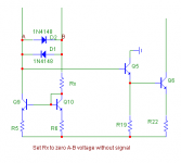
Replace Q17 with 3 pieces 1N4148 in series, first anode to base Q5, last cathode to -Ve(or with one LED with forward voltage about 1,8-2V). Or much better (for fast recovery and against "sticking") is something like attached picture
Attachments
Last edited:
If you have any recommendations as towards parts it would be appreciated.
The pnp @ digikey is £12 and free if over £50. I can bump it up to £50 quite easily, but I'd be annoyed if it turned out I'd be better off using something else etc.
I don't mind buying a few more extra transistors of different spec to 'try out' so to speak, so if you've got any personal preferences towards certain devices please say so. This can be for any part of the amplifier also. Reading Self has made me aware that the 5551/5401s aren't exactly perfect either and that a higher hFE component would be nice on the input stage.
Very suitable for VAS is 2SA1209/2SC2911, available at Profusion plc, Audio Semiconductors and Components .
Attachments
Thanks for the suggestions + places to buy from. I managed to find everything I wanted (almost) at Mouser and for very reasonable prices. The transistors were incredibly cheap.
Rapid, RS and Farnell I already use. Farnell surprised me by not having most of the things I wanted.
Profusion I have used in the past for MOSFETs I don't know why they didn't occur to me this time around 🙂 Although their website seems broken at the moment, I can get to the main page but can't look at any specifics.
With the new transistors in we get.

This is a bit under 80v p-p into the 9.4 ohm load.
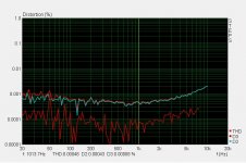
Rather brilliant 2nd, 4th & 6+ harmonics. 2nd harmonic is at only 0.002% by 10 khz.
Third harmonic, on the whole, remains unchanged. Flat line 0.0027% From 20hz up to where the sample frequency cuts off. Although it is showing a slight rise towards high frequencies. However don't confuse the 3rd harmonic with the THD plot. The rising 2nd starts to influence the THD causing it to break away a bit from the 3rd.
The new transistors, at least to my eyes, appear to be doing something good, the 2nd harmonic dropped down significantly.
Damned 3rd harmonic!
I am going to try a different PCB design, with provisions for trying out various ideas. Any suggestions?
This is a bit under 80v p-p into the 9.4 ohm load.
Rather brilliant 2nd, 4th & 6+ harmonics. 2nd harmonic is at only 0.002% by 10 khz.
Third harmonic, on the whole, remains unchanged. Flat line 0.0027% From 20hz up to where the sample frequency cuts off. Although it is showing a slight rise towards high frequencies. However don't confuse the 3rd harmonic with the THD plot. The rising 2nd starts to influence the THD causing it to break away a bit from the 3rd.
The new transistors, at least to my eyes, appear to be doing something good, the 2nd harmonic dropped down significantly.
Damned 3rd harmonic!
I am going to try a different PCB design, with provisions for trying out various ideas. Any suggestions?
Well I've made another channel with a few different options for component positions.
The first thing I've had to overcome is getting the two channels to work together in a satisfactory manner. This has given me an extra appreciation for power amp design.
Having the two channels connected together in the same way created a loop between the signal grounds that caused the distortion to deteriorate significantly. However it didn't result in a large increase in traditional hum.
We're talking both channels being capable of 0.0003% THD at 1khz (lowish power before the 3rd harmonic problem occurs), then degrading down to 0.01% for one channel and 0.005% for the other.
The problem was somewhat bizarre. I'd have one channel connected up to the dummy load and the spectrum analyser and I'd be looking at 0.0003% THD. The other channel meanwhile would be powered up, but the output from the preamp would be disconnected, ie no input connected to the other channel. Simply by connecting the grounds together from the preamps output and the amps input caused the THD to rise up to 0.01%.
To overcome this I had to connect both the input phono sockets together, ie both the grounds together, rather then being separate. Both the shielded cables connect via their shields to this common ground point at the sockets. The cables then going to their respective boards, where the signal hot and signal grounds connect to their respective points on the PCB.
This was only half the battle though as the input ground also needs a connection back to the star ground.
Having two separate wires from each amp channel back to the star ground created the same degradation in performance. Connecting only one amplifier channel to the star point was half successful. The channel connected to the star point had 0.0003% THD, however the other channel didn't fair so great, although better then before.
To solve this completely I had to take a wire from the star point back to the common ground on the input connectors - the signal ground on the PCBs connecting to the star point via the shield of the input cable.
This seems to go slightly against how I've read you should connect things, but here it works. Both channels show 0.000x distortion, this remaining unchanged if the other channel is driving a load or isn't. It's going to be interesting to see if this holds up with 6 channels in the same case!
It's times like this you appreciate you're measuring equipment for what it can do. Without it you'd be entirely oblivious to any problems hooking up the ampflier boards may have. And you're certainly not going to arrive at 'Blameless' performance without being able to measure everything each step of the way.
Instead of chasing the 3rd harmonic I decided to actually listen to the amplifier. Mono is always a disappointment and now I've got stereo I couldn't resist.😀
My main speakers are active (hence the 6 channels) so I had to 'make do' with a small stand-mount I designed a few years back. Scan D2905/95 tweeter and the old peerless 6.5" HDS polyprop sandwich cone with phase plug (850467). Xover at 2k in a small ported enclosure. All things considered they sound great, the only thing they really lack is deep bass, I could easily live with them as my main loudspeakers - they don't do anything wrong. Although I would probably want to add a sub.
To cut a long story short the amps sound sublime. And if I had to say, significantly better then with the Slone PCB.
The power levels I am using these at wont even excite the raised third order problem. I'm more interested in exorcising the 3rd order in a bid to find where it's coming from.
Currently the amps are built with FJV992/1845 on the input stage and current mirrors. F grade on the 992 and U grade on the 1845.
The VAS transistor is the aforementioned SC3503 E grade with the EF, the E grade version of the KSC1845.
They really do sound fantastic, which is nice to hear.
Now to try and hunt down the 3rd harmonic.
This is interesting as it's the only thing I've got to go on and the only thing that has actually made any difference.
It's my understanding that at low frequencies the input stage and VAS distortion is swamped by non-linearities in the output stage. This is providing the input stage and VAS are appropriately designed.
The input stage and VAS don't have any heat sinking and, as far as I am aware, operate in Class A. The current draw through the devices should therefore remain constant and hence the temperature of the devices should not change much during operation.
Whilst sat, pondering, I was watching the spectrum analyser with the amplifier giving close to full output into the 9.4 ohm load. I couldn't help but notice the THD % falling as time went on. Remember here that the THD is dominated by the 3rd harmonic.
What started out at 0.0043% fell to 0.0033% as the amplifier warmed up.
The only devices that see a temperature change during operation are the pre drivers/bias and the output transistors.
I can appreciate that the parameters of the pre drivers/output transistors could change a bit as they warm up and hence they present a different load to the VAS. If the VAS was the cause of the distortion then the change in load could explain why the distortion changes. However on the flip side I could also say that altering the parameters of the VAS transistors, to something inherently better suited made zero difference.
The strength of the emitter-follower/darlington style VAS is increasing it's linearity via increasing the apparent beta of the paired transistors.
Changing the EF and VAS transistors from two relatively low beta transistors to a pair that would have a significantly larger combined beta should, at least to my understanding, affect the VAS performance. As it's done nothing to affect the performance of the amplifier I'm tempted to say that the VAS isn't the problem.
As the load the input stage drives doesn't change a jot with time, ie the VAS doesn't heat up or cool down, then I'm assuming that the input stage isn't causing the distortion either.
I let the amplifier cool down a bit, turned it back on and wham, the distortion has risen back up to 0.0040%. Electric fan heater in hand I warmed it quickly back up again and down the distortion went.
Obviously things should sort of change as it gets hotter, but that's an output stage phenomenon via the thermal tracking.
If the output stage is truly not the cause of the increased 3rd harmonic, then some other stage would be dominating the picture. Or if looked at from another angle, the output stage's contribution (not being dominant) is so far down in level, compared to the dominant factor, that small changes in the thermal tracking should not really present themselves. In other words the thermal tracking might cause a shift from 0.0005% to 0.0008% or so as the amp warmed up. But as something else is producing 0.004% this variation wouldn't be noticed, however it is.
Also when the amplifier is driving no load and is cold the distortion is back up at its 0.004% figure. If I artificially warm it up the distortion falls back down. Note that this takes time. The input stage and VAS transistors should heat up very quickly, having very little thermal mass, so I doubt it's them.
To me, this looks like we've got a problem with the output stage.
Would anyone with more experience care to comment? Is my reasoning decent enough? Or am I missing something fundamental?
I wonder if you are detecting the change in distortion as the bias requirement for minimum distortion changes with temperature?
What happens if you increase the output bias slightly and test again with the output bias reduced slightly. Maybe +-10% from your present bias value.
Would changing the driver emitter resistor show a change in distortion?
What happens if you increase the output bias slightly and test again with the output bias reduced slightly. Maybe +-10% from your present bias value.
Would changing the driver emitter resistor show a change in distortion?
You wrote, distortion (third harmonics) is mostly level dependant (not load), at certain input level it is abrupt increasing. Try to measure distortion just behind input caps C1+C2..And try remove (bypass) C1 and use only C2 (+ pole to base Q1).
The open loop gain of the amplifier should increase with temperature, as the current gain of *all* transistors increases 🙂
You wrote, distortion (third harmonics) is mostly level dependant (not load), at certain input level it is abrupt increasing. Try to measure distortion just behind input caps C1+C2..And try remove (bypass) C1 and use only C2 (+ pole to base Q1).
I thought of this before and measured the distortion after the input caps. It didn't turn out to be the cause.
Attachments
- Status
- Not open for further replies.
- Home
- Amplifiers
- Solid State
- Slones 11.4 'Blameless'