Eureka!
And what solved the problem? Changing the 10k resistor in the feedback network.
I was browsing Farnell and I noticed that the normal super saver 1206 1% 0.5 watt buy 50 a time, surface mount resistors that I buy were rated at 50 volts. This hadn't even crossed my mind as being a source for the distortion. I didn't figure that resistors really cared about the voltage they were given - unless they were going to be exposed to very high voltages.
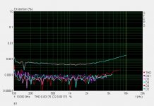
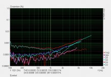
Anyway, attached are two pictures showing the distortion with no load and then with the 9.4ohm load at almost 80v p-p.
I'm glad it turned out to be something like this, because quite frankly it wasn't making much sense.
And what solved the problem? Changing the 10k resistor in the feedback network.
I was browsing Farnell and I noticed that the normal super saver 1206 1% 0.5 watt buy 50 a time, surface mount resistors that I buy were rated at 50 volts. This hadn't even crossed my mind as being a source for the distortion. I didn't figure that resistors really cared about the voltage they were given - unless they were going to be exposed to very high voltages.
Anyway, attached are two pictures showing the distortion with no load and then with the 9.4ohm load at almost 80v p-p.
I'm glad it turned out to be something like this, because quite frankly it wasn't making much sense.
Attachments
Excellent! Good for you.
Great thread with great documentation, explanations and a mountain of usefull information.
Great thread with great documentation, explanations and a mountain of usefull information.
Excellent! Good for you.
Great thread with great documentation, explanations and a mountain of usefull information.
ditto
regards Max
Thank you kindly. 🙂
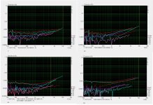
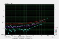
And just for completion here's the distortion plots for all 4 channels, same order as the last one. They are all driving the 9.4 ohm load at just under 80v p-p.
They all perform well, with perhaps no 1. taking prizes for the best. Either way at distortion levels this low small differences in the position of wiring can alter things quite dramatically, so it's hard to say if it's really the PCB itself that's causing the differences.
No.4 is the worst out of the lot and I think this is because I put some traces and the one component on the copper bottom. I feed the +ve and -ve power into the boards via a twisted cable that connects to the copper bottom. Moving the power cable around a bit changes the performance quite dramatically, so for the remaining boards I will certainly move those traces back to the top.
Attachments
well done.
It's usual to run the feedback resistor at <<50% of it's power rating.
Your 10k was only dissipating 16% of 500mW rating. Surprised that it showed up as badly as it did.
Are you sure 1206 is 500mW?
The Truohm 1206 that Rapid sell are 250mW, 200Vrms.
It's usual to run the feedback resistor at <<50% of it's power rating.
Your 10k was only dissipating 16% of 500mW rating. Surprised that it showed up as badly as it did.
Are you sure 1206 is 500mW?
The Truohm 1206 that Rapid sell are 250mW, 200Vrms.
well done.
It's usual to run the feedback resistor at <<50% of it's power rating.
Your 10k was only dissipating 16% of 500mW rating. Surprised that it showed up as badly as it did.
Are you sure 1206 is 500mW?
The Truohm 1206 that Rapid sell are 250mW, 200Vrms.
MULTICOMP|MCHP06W2F1002T5E|RESISTOR, 10K, 1206 1% 0.5W | Farnell United Kingdom
Was the offending article.
Multicomp also do another version that's rated at 200 volts, but can only dissipate 125mW. I wasn't really expecting the resistor change to do anything, then I fired up the spectrum analyser. This can't be right, I thought, I've got the scope on the wrong voltage setting or something, but nope, there it was.
I've got two extra boards now etched and ready for drilling. Once I've got 6 made I can try them out with the proper system.
It is nice to finally solve the mystery.

40Vpk across 10k dissipates 80mW.
Use smaller devices, like 125mW or 250mW, by paralleling multiples. eg 4off 51k and 1off 47k = 10k1 & the 47k runs @ <14% of 125mW.
What you don't need is temperature modulation in the feed back circuit.
Use smaller devices, like 125mW or 250mW, by paralleling multiples. eg 4off 51k and 1off 47k = 10k1 & the 47k runs @ <14% of 125mW.
What you don't need is temperature modulation in the feed back circuit.
Last edited:
Congratulations!
Thanks😀 It's nice to finally solve the problem, as much for myself, as for here.
40Vpk across 10k dissipates 80mW.
Use smaller devices, like 125mW or 250mW, by paralleling multiples. eg 4off 51k and 1off 47k = 10k1 & the 47k runs @ <14% of 125mW.
What you don't need is temperature modulation in the feed back circuit.
Indeed, I had thought about paralleling some of the SMD devices up. At this time it was easier to use the through hole components I had.
I'll have the other two channels built later on today and I'll measure and post their results too.
It was not about thermal modulation (frequency independent, no thermal inertia) but about "voltage modulation", so paralleling can not help. You should use resistors with appropriate allowed voltage rating.
Last edited:
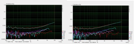
As promised here are the distortion plots for the last two channels of the 6 channel amplifier. Nothing surprising here.
And for completeness, here's also the amp driving 120 watts into the 4.7 ohm load. I can squeeze 140-150 out of it before clipping, but at that point the distortion deteriorates down to around -85dB, still decent enough. A 2.35 ohm load? No, thank you!
The most immediate improvement over the previous 6 channels is the noise level. There's less hiss and far less low level 'buzz/hum' then with Slone's boards. This is most likely down to proper grounding within the entire amplifier and I'm pleased with that result. The noise the system produced always irritated me and I had always assumed it the fault of the active xover, but it appears that the amp was as much to blame.
At some time I will end up posting a picture of the 6 channel amp and describe how I wired it up so that the channels don't 'talk' to one another via messy grounding. I did give a small description before, but that was most likely hard to follow and even if my MS paint skills are nothing to be proud of a picture would probably be very helpful.
Attachments
Hi,
a good 8ohm capable power amp should be able to drive a resistive 2r6 load for at least a few seconds, if started from cold heatsinks.
A good 4ohm capable amplifier should be tested into 1r3 for at least a few seconds.
If it oscillates or suffers severe output voltage limiting or triggers protection circuits then something needs sorting.
Earlier you said the first PCB showed better performance. Has that opinion changed or does it depend on what parameter is being assessed?There's less hiss and far less low level 'buzz/hum' then with Slone's
Last edited:
Hi,
a good 8ohm capable power amp should be able to drive a resistive 2r6 load for at least a few seconds, if started from cold heatsinks.
A good 4ohm capable amplifier should be tested into 1r3 for at least a few seconds.
I'll try giving this another go, currently the amps are in a system elsewhere in the house so I can't measure anything.
Earlier you said the first PCB showed better performance. Has that opinion changed or does it depend on what parameter is being assessed?
I think there's been a misunderstanding. When I referred to the first PCB in post 124 I was referring to the first PCB I created. Slone's PCBs were the ones that hissed/buzzed.
I previously had 6 channels of Slone's design and with those in the system the noise level present on the loudspeakers was always higher then I liked.
With 6 channels of my PCB the noise level is far lower, you cant even hear it unless you go pressing your ears up to the drive units.
Here's the inside of the amp. 😀
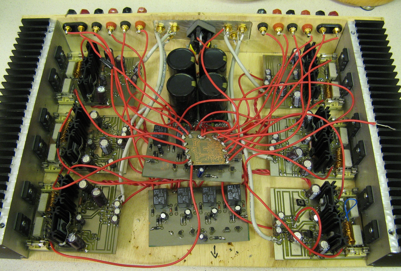
A fine example of organised chaos if I do say so myself.
But it does show at least, that you can arrive at 0.000x% THD between channels without any significant degradation in performance via, what Self calls, Induction or Rail decoupling distortion.
For example one channel driving 1khz into no load at 80 volts p-p would have 0.00035% THD. If another channel is asked to do the same, however this time driving a 9.4 ohm load, the performance of the first channel decreases to 0.00045%. There is some coupling but nothing that's any cause for concern.
The bridge rectifier is mounted in the middle of the input connectors, this doesn't appear to do anything to harm the performance.
Grounding.
The first thing to mention is the aluminium plate at the back of the amp. All of the input connector grounds are connected together via this.
From this point shielded cables are taken to the individual amplifier boards. The screen is connected to the aluminium plate, then at the other end connected to the signal ground of the amplifier.
In this case R4, D1 and C7 are the only things that make up the signal ground.
R9 connects to -ve instead of ground as recommended by Andrew, with R8 and R9 increased in value to 20k.
From the metal plate 1 wire is taken to the star point.
The amplifier boards have a separate connection for power ground. This is made up of C3, C4, C11, C12 and the ground connection of Q5.
Connecting Q5 to either the signal ground or power ground didn't change the performance. In the final board design it was easier to connect this to the power ground, but either will do.
After the bridge rectifier are the smoothing caps. These are soldered to a PCB. The PCB is made from 2oz copper with a fat trace down the middle of it creating a ground point. I've taken two wires from this fat trace, back to a separate piece of PCB that I am using for the star ground point.
The ground return for the relays and the power ground from the amplifier boards are taken back to the fat trace on the smoothing cap PCB.
The ground connection for the output and the zobel connect back to the star ground.
C6, C9 and C10 are NPO/COG and should have a voltage rating capable of handling the output swing of the amplifier.
The heat sinks on the pre drivers are 10 degree/watt SW38s and get slightly warm to the touch in use.
I ended up using SC5200/SA1943s for the output transistors. Some are genuine ones from Toshiba, the others are from Magnetek, both perform as well as each other in this application.
2SD669/SB649 are used as the pre drivers and the bias tracking transistor.
The input and current mirror transistors ended up being FJV1845/FJV992. U spec for the 1845s and E for the 992s. Mouser didn't have any 992s in the U specification.
The VAS transistor (Q6) is a 2SC3503 of the E variety. The emitter follower (Q5) is a KSC1845 of the E variety also.
All the other transistors are the same as the schematic in post 16.
The PCB layout of post 40 is slightly different to the design I ended up with, but as shown in post 124 it works very well.
Andrew the amps can deliver about 55 watts into a 2.35ohm load.
Last edited:
Was reading though this thread and noticed your resistor problem, a tip: Use only thin film smd resistors in critical audio path, preferable Susumu, available at Digikey.
Soren
Soren
Was reading though this thread and noticed your resistor problem, a tip: Use only thin film smd resistors in critical audio path, preferable Susumu, available at Digikey.
Soren
good point!
Hat off 5th element!
impressive work and patience that you invested here.
funny that such a small component can make such a difference, perhaps using a TH 0207 reaiator for this one is safer, because they have much higher voltage ratings.
years ago I built several blameless modules as well, but all with TH components and it was an early version with EF2 output stage instead of CFP. they're still running seamless.
you have a nice measurement tool, the Neutrik A2 I can use doesn't support individual distortion components like yours. need to think about investing there... 😉
about your 'organised chaos', I mean once the cover is closed nobody will see that and finally the performance is what counts.
nice one!
jvo
Hat off 5th element!
impressive work and patience that you invested here.
Thanks 🙂
funny that such a small component can make such a difference, perhaps using a TH 0207 reaiator for this one is safer, because they have much higher voltage ratings.
It is indeed and I learned the hard way, but rest assured I wont forget it in a hurry!
I assume you are referring to these. As I am in the process of getting a higher powered version of these built, I certainly want to make sure that the same thing doesn't happen again.😀
you have a nice measurement tool, the Neutrik A2 I can use doesn't support individual distortion components like yours. need to think about investing there... 😉
It's nothing special really, just a high performance DAC/ADC hooked up to the PCI interface chip on an M-Audio sound card.
The simplest way to get similar performance would most likely be an Asus Xonar card of some sort.
Stereophile measured one here and it's certainly up to the task.
about your 'organised chaos', I mean once the cover is closed nobody will see that and finally the performance is what counts.
Indeed. I think its a hidden inevitability with DIY, that no matter how much care you take, you will always end up with spaghetti junction inside the box 😀
Was reading though this thread and noticed your resistor problem, a tip: Use only thin film smd resistors in critical audio path, preferable Susumu, available at Digikey.
Soren
Farnell stock a wide range of Susumu resistors also. It would seem that for the resistor in the feedback network that a MELF resistor, such as vinyljvo suggested might be a better bet. The Susumu's that Farnell stock don't really go up high enough in voltage and also can't handle quite enough power.
Yeah, the MELF part is also thin film, I'm just always thinking about automated assembly and therefore don't like round parts....
The Susumu 1206 is specified for 150V and 0.25W.
I prefer Digikey over Farnell, better stock, better pricing and better website. They stock the 1206 Susumu but in the more expensive 0.1% version....
The Susumu 1206 is specified for 150V and 0.25W.
I prefer Digikey over Farnell, better stock, better pricing and better website. They stock the 1206 Susumu but in the more expensive 0.1% version....
- Status
- Not open for further replies.
- Home
- Amplifiers
- Solid State
- Slones 11.4 'Blameless'