Sorry if I'm repeating what's been said before, but I built a Load Invariant "Blamless" amp with the following grounding approach (mostly similar to what I remember reading earlier):
Separate ground networks for power ground and signal ground. The two grounds are separated by a 10R resistor but, after routing, I think it can just as well be 0R. The 0V reference point of the signal ground is close to the 10R separating resistor, and the 0V reference point of the PCB power ground is close to the other side of same resistor. My proposed take-off point for the loudspeaker ground is on the board. It works, taking it from the usual PSU reservoir star point, of course, but I'd like to know whether my grounding idea might yield a better result; the idea being that the sensing points (to steal a term from instrumentation field) are as close to the load as on-board sensing will allow.
Separate ground networks for power ground and signal ground. The two grounds are separated by a 10R resistor but, after routing, I think it can just as well be 0R. The 0V reference point of the signal ground is close to the 10R separating resistor, and the 0V reference point of the PCB power ground is close to the other side of same resistor. My proposed take-off point for the loudspeaker ground is on the board. It works, taking it from the usual PSU reservoir star point, of course, but I'd like to know whether my grounding idea might yield a better result; the idea being that the sensing points (to steal a term from instrumentation field) are as close to the load as on-board sensing will allow.
Sorry if I'm repeating what's been said before, but I built a Load Invariant "Blamless" amp with the following grounding approach (mostly similar to what I remember reading earlier):
Separate ground networks for power ground and signal ground. The two grounds are separated by a 10R resistor but, after routing, I think it can just as well be 0R. The 0V reference point of the signal ground is close to the 10R separating resistor, and the 0V reference point of the PCB power ground is close to the other side of same resistor. My proposed take-off point for the loudspeaker ground is on the board. It works, taking it from the usual PSU reservoir star point, of course, but I'd like to know whether my grounding idea might yield a better result; the idea being that the sensing points (to steal a term from instrumentation field) are as close to the load as on-board sensing will allow.
Thanks again.
I understood what you meant the first time around. But I've got two separate grounds for both power and signal. The constant current source grounds are connected to the signal ground, but Self says that this is fine as they inject such a small amount of current, that is also constant, into the ground itself. The ground connection from the emitter follower VAS I've tried on either the signal or the power ground and it makes no difference.
As it stands the power ground simply carries the ground connection for the decoupling caps, as recommended by Self, and has a separate return back to the star point.
I have been thinking about re-routing the grounding. First continuing the signal ground as a thick trace down the middle of the board beneath the feedback take off point trace. One end has the signal grounds connected to it at the input stage and the other end, after it's run beneath the feedback trace I use as the return path for the -ve speaker connection.
I am unsure though as to if this would be a wise idea in my current situation, as the loudspeaker return would run down the shield of the input cable before returning to the star point. I can't imagine that this would be a good idea.
I don't suffer from any of the usual problems with regards to bad grounding either. I can try wiring the constant current source return path into the power ground, but I doubt that would do anything.
or keep the CCS currents out of the ground and return them to the opposite supply rail. Double the resistor value, or keep the existing resistor value and add a series connected jFET CCS from the opposite rail (check the FET voltage limit).
Thanks again.
I understood what you meant the first time around.
I guess that means I've posted this earlier on in the thread already
 . I was actually referring to what someone else might have said, not realising that I had indeed done so. Hehe.
I like that you have very good measured performance right now, and are still trying to understand how to reduce it further. Keep at it.
I guess that means I've posted this earlier on in the thread already
Maybe I misunderstood what it was you originally said then!😀
I like that you have very good measured performance right now, and are still trying to understand how to reduce it further. Keep at it.
That's basically it. The performance is perfectly acceptable for actual use, it's just that I'd rather like to find out where that third harmonic is coming from.
or keep the CCS currents out of the ground and return them to the opposite supply rail. Double the resistor value, or keep the existing resistor value and add a series connected jFET CCS from the opposite rail (check the FET voltage limit).
That's actually a nice idea. It sims well so I'll give it a go and see what I get (with resistors that is).
That's actually a nice idea. It sims well so I'll give it a go and see what I get (with resistors that is).
I tried this, I rather liked the idea as removing stuff put into ground has to be a good thing. Unless of course you end up with more stuff injected from the rails.
The overall performance didn't really change.
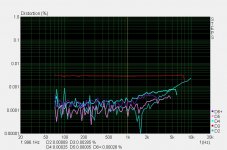
Attached image is at full power into 9.4 ohms. All the faffing about with the test equipment did allow me to improve the situation a little, although I'm sure this could just be down to a little harmonic cancellation.
For instance the left and right inputs to the ADC give slightly different results and lifting the ground also changes the 2nd harmonic. Nowt much changes the third harmonic though, its always prominent.
Having added a VAS buffer to no positive effect and moving things around on the PCB, I'm generally getting no seeing no real changes. Great performance from everything but third harmonic.
I've fiddled around with the input stage, nothing changes, I've messed around with the VAS and again no changes. I've altered the layout in places and this hasn't affected much either.
In the version with two separate current sources applying a cap from the base of Q8 to the +ve rail does anything, this is anything good or bad, it does nothing at all. I've tried a 2n5401 in place of the 649 too and this didn't to anything.
This wouldn't be something stupid like the fact I've got the transistors mounted with full leg length -.- I could solder them much closer to the boards.
Attachments
Do you have an aggressive circuit board cleaning chemical? I would be interested to know if you find any difference in performance after board cleaning.
I have recently redrawn the PCB for the 11.4 amplifier, guided by some of Douglas' groundind technics, and also other minor improvements.
This is what I ended with:
The construction notes, schematics, BOM, along with the layout, can be foud here: http://www.nabucoeletronica.com.br/files/slone-mods-by-Nabuco.pdf
I would really appreciate your comments!
Thank you,
This is what I ended with:
An externally hosted image should be here but it was not working when we last tested it.
The construction notes, schematics, BOM, along with the layout, can be foud here: http://www.nabucoeletronica.com.br/files/slone-mods-by-Nabuco.pdf
I would really appreciate your comments!
Thank you,
Do you have an aggressive circuit board cleaning chemical? I would be interested to know if you find any difference in performance after board cleaning.
Eh? Nowt but copper and the photo-resist layer on top of the tracks, which I leave there to prevent corrosion. After I've done drilling and the final cutting/filing to shape I was the boards in hot soapy water. What is it you think the boards have on them?
I have recently redrawn the PCB for the 11.4 amplifier, guided by some of Douglas' groundind technics, and also other minor improvements.
This is what I ended with:
An externally hosted image should be here but it was not working when we last tested it.
The construction notes, schematics, BOM, along with the layout, can be foud here: http://www.nabucoeletronica.com.br/files/slone-mods-by-Nabuco.pdf
I would really appreciate your comments!
Thank you,
Okay.
I'll say what I see, others can correct me if I'm talking cods-wallop.
First of all you do not need heat sinks on Q8,Q5 and Q6. They are barely even warm to the touch, so save your pennies!
You've separated out the power and signal grounds in a decent enough way, this is something that Slone's board severely lacked in.
*Q5, Q6*– *mounted back to back on the same heatsink.*Should*be matched in Hfe and Vbe.
This is not important, in fact these two devices don't even need to be of the same type. This is one area where Slone's transistors could be improved upon. If you read the rest of this thread you will see recommendations for the parameters of Q5 and Q6.
Q1, Q2*– *mounted back to back. Should be tied together and matched in Hfe and Vbe.
This is a good idea as it will help reduce thermal drift effects on the DC offset. Matching Hfe will keep the pair balanced, reducing DC offset again and ensuring good cancellation of 2nd order from the input pair.
Q9, Q10*– *mounted back to back on the same heatsink. Should.be matched in Hfe and Vbe.
Q9 and Q10 do not need a heat sink. Matching Hfe should help to keep DC offset low. In practise though I don't think this is that important. You should be able to easily get below 5mV DC offset with a well matched input pair.
Q11, *Q12,*Q13,*Q14*–*Mounted on main heatsink.* Q7*–*mounted on a small thermal bar, made of aluminum or copper, wich should be screwed to the front of Q12 ans Q14.
This is the main problem. This amplifier uses a complementary feedback output stage. Q7 is required the thermally track Q11 or Q13 not the output pair.
As you will see in my design, Q11 and Q13 are mounted to individual heat sinks, with Q7 mounted directly on top of Q11.
This is one area I disliked about the Slone PCB. In effect I don't think having Q11-Q14 + Q7 mounted on the main heat sink would decrease the overall performance by that much. However it's a royal pain in the behind to fasten each transistor + thermal pad to the main heat sink, and makes it a pain if you ever need to remove the amplifier from the heat sink. Having only the output pair attached makes this far easier.
You've changed the input filter, I think you still need to make sure to maintain balance between R4 and R10.
The feedback take off point is ill-advised and I dislike Slone carrying the output of one of the RE resistors through a wire link.
You also have C13 from the zobel returning through the power ground, I don't know if this will do any harm. I definitely can tell you that my amplifiers need the zobel for stability, I tried removing it and they were not happy.
Eh? Nowt but copper and the photo-resist layer on top of the tracks, which I leave there to prevent corrosion. After I've done drilling and the final cutting/filing to shape I was the boards in hot soapy water. What is it you think the boards have on them?
As I read through the thread from the beginning, I didn't find anything wrong with your approach or the suggestions. I really couldn't think of anything to add which might be helpful. Then I saw where you compared your amplifier with another which did not exhibit the distortion and I got to wondering about production/manufacturing issues. Could there be something about your board-making process that leads to your distortion?
When I visit the subs who do my board assembly, I get the tour, see the new machines and inspect the production lines. They always seem to stress the board cleaning, they show me how its done. I admit, I have not done my homework on chemicals, so I just stand there and nod my head looking thoughtful. I don't know much about this, except that in the last few years they had to change from nasty chemicals to enviro-friendly cleaners.
I don't have any particular culprit in mind, just wondering if there could be a difference due to manufacturing materials and technique, and that made me wonder if anything physical could lead to your distortion. I considered asking about your board materials, solder, and so forth, but then remembered a board cleaning problem we had. We were testing a new product which had multiple DAC channels, and on one test board we were chasing offset drift. Nothing on that board was different from the others, and the drift would come and go, sometimes this channel, sometimes over there, we probed and probed and heated and cooled and never found anything causative. Then somebody remembered that this board had gone back for rework, something hadn't passed inspection. So we sent it back to be recleaned...and that did it, the drift was gone.
When you said "That leaves the PCB. Throw any ideas at me." That's what I did, I just threw the idea at you.
When you said "That leaves the PCB. Throw any ideas at me." That's what I did, I just threw the idea at you.
😀
I have read that the flux used within certain types of solder can dissolve copper traces over time. This is certainly not a good thing! and is reason enough for some people to clean their boards after they have been soldered up. The faulty board could quite easily have had a thin film of something somewhere, in the wrong place that could have caused this problem.
I have used the same board manufacturing process to make the PCBs that house the DACs/ADC that I'm using for the measurement process. If something was going to show up, I would more expect it to be there perhaps then with the amplifiers.
This is one very interesting thread, it should be read by by anyone interested in building the Lin topology amps, this is how one learns how to build a proper functional amp to get maximum performance out of it, my hats off to 5th element.
Indeed!......... it should be read by by anyone interested in building the Lin topology amps, this is how one learns how to build a proper functional amp to get maximum performance out of it, my hats off to 5th element.
This is one very interesting thread, it should be read by by anyone interested in building the Lin topology amps, this is how one learns how to build a proper functional amp to get maximum performance out of it, my hats off to 5th element.
Indeed!
Now you're making me blush and I noticed we don't have a blushing smily, so I'll use this one instead

Part of the goal was to catalogue the changes here so anyone else can maybe learn something from it. I've certainly taken a lot from many other threads here on DIY, so I figure I should try giving something back😉
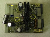
One of the things I did try out on the second board was as the awful picture shows.
For example I could either place the components that connect from the power lines, either at the power lines (yellow arrow), or close to the input/VAS stages (black arrow). When the real resistor was put near the black arrow I used a 1.5R resistor at the yellow arrow.
Also I made provisions for having part of the feedback network wired up either near the output stage or near the input stage.
Neither of these did much at all to the performance.
And yes the board/components look a little beaten😀 but that happens when you're changing components around.
Attachments
5th element said:This is the main problem. This amplifier uses a complementary feedback output stage. Q7 is required the thermally track Q11 or Q13 not the output pair
You're absolutely right, thank you! Well, I could use a small thermal bar mounted on front of Q11 and Q13, and having Q7 mounted directly over that bar. A thin aluminum or copper bar would make heat trasnfer to Q7 more efficient.
Would you recommend that? I have already etched the boards, so I'd like to use them...
5th element said:The feedback take off point is ill
I'm sorry, I don't understand what you meant, could you say what's wrong?
5th element said:You also have C13 from the zobel returning through the power ground
I can separate that from power ground and run a separate return to HQG instead. Would you think it's worthy?
Thank you very much my friend, you've been of great help. 🙂
You're absolutely right, thank you! Well, I could use a small thermal bar mounted on front of Q11 and Q13, and having Q7 mounted directly over that bar. A thin aluminum or copper bar would make heat trasnfer to Q7 more efficient.
Would you recommend that? I have already etched the boards, so I'd like to use them...
There's no harm in giving it a go. Ideally you should have Q7 mounted directly on top of Q11 or Q13. You could attach wires to Q7 and have it mounted free from the PCB, that way you could attach it directly to one of the pre drivers.
I'm sorry, I don't understand what you meant, could you say what's wrong?
Feedback works by taking a portion of the output signal and feeding it back into the input. The two signals are then compared and anything the amplifier can do to get them as close to being equal as it can, it will do.
In this sense it's vital that the feedback signal be as accurate a representation of the output as is possible. If some grunge gets into the feedback and contaminates the signal, the comparison is now flawed and hence the performance suffers.
The junction between the RE resistors R33 and R34 is the point where the output from the positive and the negative side of the amplification process are summed. This specific point, according to Self, is a turbulent place to be and I guess you could sort of liken it to the junction between two reservoir capacitors in the power supply. You don't connect anything to that junction, but take a tee off of it and this point is used as the HQSG, or in this case used as the output of the amplifier.
You then take the feedback off of this point too, but slightly before the output inductor.
Slone has the feedback point at one side of the RE resistors, before they've summed, this is wrong. In fact he connects the output from one of the RE resistors through a wire junction J4 in your schematic. The start of the feedback take off circuit is C6 R11 and R10. Follow the trace common to R10 and C6 and follow it back toe J4, that's the feedback take off point Slone has used.
Slone has to use this junction because he's got the traces from Q7 running down the middle of the board. If you were to attach Q7 to individual wires instead, you wouldn't need this junction and you could redesign the output and junction between the RE resistors in a much better way.
I can separate that from power ground and run a separate return to HQG instead. Would you think it's worthy?
It might help, I don't really know. You'd need to measure the amp to determine if it was needed. It certainly wouldn't hurt to have a separate connection back to the star point.
So now I've got 4 channels built.
In the 4th iteration I went back to the combined current source for the VAS and input stage. Separating them out appeared to do virtually nothing to solve the third order problem.
I also altered the case that would eventually hold the 6 channel version. This allowed me to wire up the 4 channels together, rather then only being able to wire up 2 as per the other chassis. Like this I measured each version one after the other and plotted their distortion performance next to each other. These were all taken close to 80v p-p with no load. Also the 4 channels perform as well as they did before. The wiring arrangement I'm using shows almost complete immunity between the channels. There is crosstalk, but this isn't induced or coupled via sine pulses through the grounding or from the power supply.
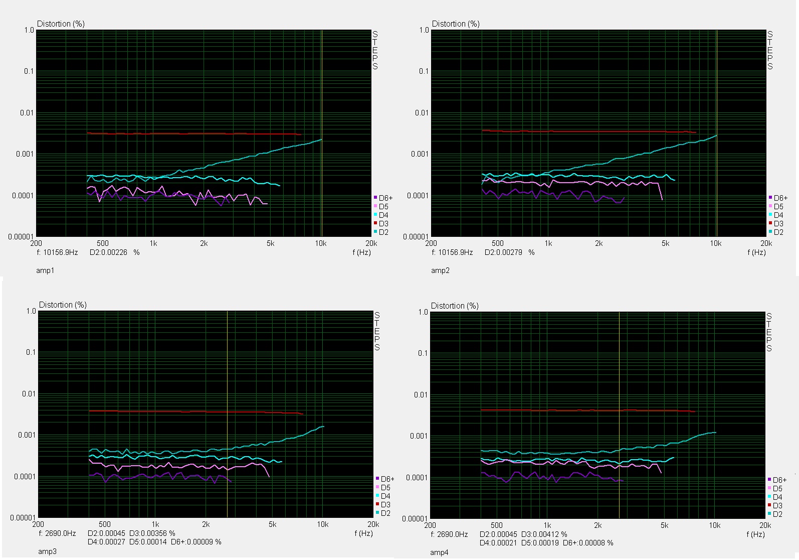
First of all the 4th, 5th and 6th+ harmonics are comfortably low enough down for all of the 4 channels. There's a bit of variation, but I'd be surprised if there wasn't.
The second order is also acceptable, even though there is a slight difference in the trend that the different channels show.
Then there's the third harmonic.
Ironically the amplifier that shows the best performance is the 1st one I built, but then there's only a small difference between the four.
Ranging from about 0.003% - 0.004%. This isn't a fluke of the measurements either. Channel 1 is consistently better then channel 4 and they both showed the same performance when in the other case too.
Channel 1 was built as is shown in the first PCB layout I posted. In this case the ground connection of the CCS has been connected to -ve power via a wire and the component values changed as Andrew suggested.
Channel 2 was identical to channel 1, except it had options to alter the position of various components - as shown in post 117 - also included was Andrews suggestion of splitting R22 into two smaller values, to provide better headroom for the VAS.
Channel 3 split the current sources and the experiment of component positions in channel 2 showed no real changes I positioned the components as per channel 1. I also placed the VAS closer to the input stage and repositioned C7, D1 and gave provisions for altering the position of R13 so that none of the components would straddle the feed from the input stage to the VAS.
Channel 4, went back to the original current source configuration. I also altered the orientation of a couple of resistors, more out of necessity then as an actual test. The through hole resistors I got from Mouser were slightly larger then I thought they would be. On top of this I placed R23 as per the first PCB schematic on the copper bottom and routed the traces from Q13>Q14 on the copper bottom too.
I am doubtful that any of these changes really affected the root cause of the third harmonic at all. Yes there is a tiny difference between all 4 channels, but it's minimal at best and could easily be down to component tolerances or slight changes between the interference of harmonics within the system as a whole.
The next thing I'm going to try is re-routing some of the traces of the input stage to see if that makes any difference.
In the 4th iteration I went back to the combined current source for the VAS and input stage. Separating them out appeared to do virtually nothing to solve the third order problem.
I also altered the case that would eventually hold the 6 channel version. This allowed me to wire up the 4 channels together, rather then only being able to wire up 2 as per the other chassis. Like this I measured each version one after the other and plotted their distortion performance next to each other. These were all taken close to 80v p-p with no load. Also the 4 channels perform as well as they did before. The wiring arrangement I'm using shows almost complete immunity between the channels. There is crosstalk, but this isn't induced or coupled via sine pulses through the grounding or from the power supply.
First of all the 4th, 5th and 6th+ harmonics are comfortably low enough down for all of the 4 channels. There's a bit of variation, but I'd be surprised if there wasn't.
The second order is also acceptable, even though there is a slight difference in the trend that the different channels show.
Then there's the third harmonic.
Ironically the amplifier that shows the best performance is the 1st one I built, but then there's only a small difference between the four.
Ranging from about 0.003% - 0.004%. This isn't a fluke of the measurements either. Channel 1 is consistently better then channel 4 and they both showed the same performance when in the other case too.
Channel 1 was built as is shown in the first PCB layout I posted. In this case the ground connection of the CCS has been connected to -ve power via a wire and the component values changed as Andrew suggested.
Channel 2 was identical to channel 1, except it had options to alter the position of various components - as shown in post 117 - also included was Andrews suggestion of splitting R22 into two smaller values, to provide better headroom for the VAS.
Channel 3 split the current sources and the experiment of component positions in channel 2 showed no real changes I positioned the components as per channel 1. I also placed the VAS closer to the input stage and repositioned C7, D1 and gave provisions for altering the position of R13 so that none of the components would straddle the feed from the input stage to the VAS.
Channel 4, went back to the original current source configuration. I also altered the orientation of a couple of resistors, more out of necessity then as an actual test. The through hole resistors I got from Mouser were slightly larger then I thought they would be. On top of this I placed R23 as per the first PCB schematic on the copper bottom and routed the traces from Q13>Q14 on the copper bottom too.
I am doubtful that any of these changes really affected the root cause of the third harmonic at all. Yes there is a tiny difference between all 4 channels, but it's minimal at best and could easily be down to component tolerances or slight changes between the interference of harmonics within the system as a whole.
The next thing I'm going to try is re-routing some of the traces of the input stage to see if that makes any difference.
- Status
- Not open for further replies.
- Home
- Amplifiers
- Solid State
- Slones 11.4 'Blameless'