I am wishing out loud that the 21st could be integrated into the output board too.😀 SMD and all...😀
Yup , but only part of it.
The DC/current protect and SS relay will be on my new OPS.
Able to be connected out to the "21'st" , but able to work independently.
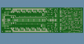
I am past frustration now with diptrace (below 1/2).
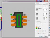
But , I am worried about these SOT23-6 pads , the 3D 23-6 does not fit
the pads , but a 363 will ??? (below 3).
I WILL get it !!
OS
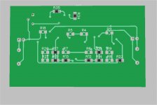
Attachments

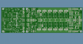
Print the design 1:1 and offer up a real device? One of my sanity checks 🙂 Then at least you can pin point where the problem is (software or design)
Paul
Paul
Did you create your own pattern, or use a preloaded one? The preloaded patterns are usually pretty good. I see you have some scaling set in the 3d model. That should be 0s.
Print the design 1:1 and offer up a real device? One of my sanity checks 🙂 Then at least you can pin point where the problem is (software or design)
Paul
I've gotten into the habit of printing the whole board and stuffing it with parts before sending out Gerbers. It always looks like there's more room in the software.
how about using BF862 for the input for KyptonV2? I agree the fact that its RF part but with gate resistors it can be stabilized. In the case of Kyptonv2 there is already 820 ohm at input and 22k as the feedback resistor. So will there be any stabilities issue?
how about using 2sk2145 but its dual with common source. So omitting source resistor would imbalance ? we still have 1k resistor at the input connecting to the source. Any chance of using 2sk2145?
how about using 2sk2145 but its dual with common source. So omitting source resistor would imbalance ? we still have 1k resistor at the input connecting to the source. Any chance of using 2sk2145?
On a basis "Sansui"The only real way is to actually make some amplifiers.
Attachments
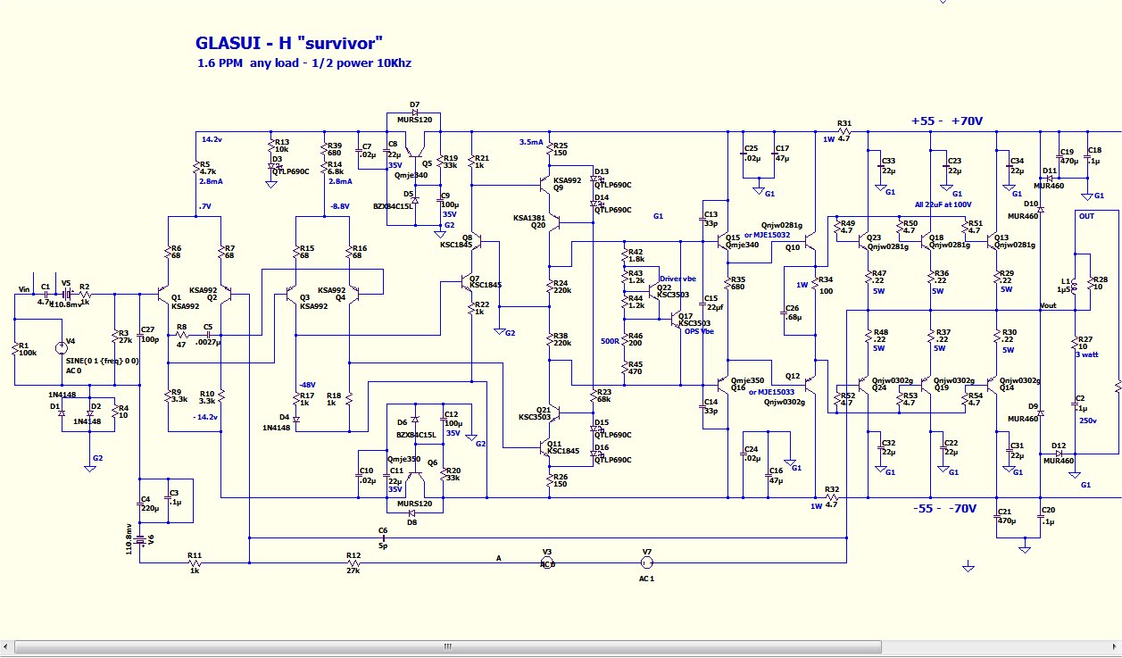
what is THD at 10Khz?
The real THD is determined by the imperfection of transistors and
magnetic fields interference from the output stages to the input. So linearity won't be as high as in the model. Usually is 0,000.2...0,000.3% at a frequency of 20 kHz at full output. Because with the decrease of the signal frequency feedback grows, it is hoped that lower range and distortion will be less than the given level.
But the focus should be on the level of 0,000.2...0,000.3%, it is practically measured.
Last edited:
I like the IPS as it has nice jfet cascode with wilson mirror this was exactly what i was planning to use.On a basis "Sansui"
Have you found any sonic benefits of using such jfet cascode? what is the necessity of using small inductor between the sources of the jfets?
Due to high input capacitance (which reduces the slew rate and depth feedback) and nonlinear characteristics of FETs in the output stage consider to be evil. 🙂 Bipolar transistors are better.
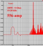
An inductor L2 between the emitter Q35 Q36 input stage (556.asc) is an element of frequency compensation. L2 and R21R23 reduce the amplification of this cascade is higher than 1.8 MHz.
An inductor L2 between the emitter Q35 Q36 input stage (556.asc) is an element of frequency compensation. L2 and R21R23 reduce the amplification of this cascade is higher than 1.8 MHz.
Last edited:
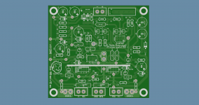
hello guys thanks this thread now I'm incorporate ideas into my practice layout works this is a mosfet amplifier from the book of G. Randy Slone page 362 🙂
I hope OS don't mind 😛
I hope OS don't mind 😛
Attachments

Now Slewmaster is school!hello guys thanks this thread now I'm incorporate ideas into my practice layout works this is a mosfet amplifier from the book of G. Randy Slone page 362 🙂
I hope OS don't mind 😛
vargasmongo3435 What rail voltages are you running those fets @?
85V
I hope that page 362 is NOT the version that uses dual CCS for the input LTP !.............. this is a mosfet amplifier from the book of G. Randy Slone page 362............
good comment!
😀
looks like it is not ...
mlloyd1
😀
looks like it is not ...
mlloyd1
I hope that page 362 is NOT the version that uses dual CCS for the input LTP !
Attachments

hold on sorry this section is for slew designs I think I should not do that, I will not post here anymore please moderators delete all about the G. Randy subjects in this section, from post number #9333 to this one # 9339
Attachments
Last edited:
vargasmongo3435
If you don't mind I can give you a small advice, so you do not have to repeat my mistakes.
I have build a few amps with latfets as in your OPS and the bias was not so stable drivers are heating up and they really need a compensation (If you will close amplifier enclosure the drift will be a way larger). So I have putted a smal BC to92 transistor to compensate drivers at the small heatsink. Now bias is rock solid no mather what.
Just a few components more and the difference is really worth it.
In between Q6 and Q7 there is a lot of room for small to92 transistor.
Regards Peter
- Home
- Amplifiers
- Solid State
- Slewmaster - CFA vs. VFA "Rumble"