Vargas , heed Bory's suggestion.
Look up the Vfet and the Lfet versions of the slew OPS.
I also don't know why you are using that 30 YO sloan input stage.
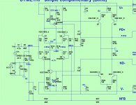
We have 2 complimentary designs available.
(spooky and symetri).
Member Still4given built both - thermally and electrically perfect.
Symetri is the best clipper and is only 10 semi's (below).
NO zener's and loves >80V rails , as well.
OS
Look up the Vfet and the Lfet versions of the slew OPS.
I also don't know why you are using that 30 YO sloan input stage.
We have 2 complimentary designs available.
(spooky and symetri).
Member Still4given built both - thermally and electrically perfect.
Symetri is the best clipper and is only 10 semi's (below).
NO zener's and loves >80V rails , as well.
OS
Attachments
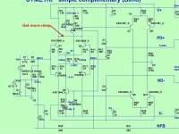
Symetri is the best clipper and is only 10 semi's (below).OS
Re-check draft schematic.
Do you also have a cascode IPS version you favor?
Attachments
Last edited:
Re-check draft schematic.
Do you also have a cascode IPS version you favor?
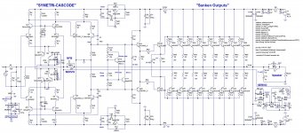
Did you consider the two factors you added (thermal) by including the
2Q CCS's and the cascodes (impedance) ?
Edit - yes , the original spook ..... cascoded LTP = the cascoded hawksford (thermally).
5.25ma @ 0C to 5.19ma 40C VAS I.
OS
Last edited:
how much idle current per transistor for KyptonV2 is recommended. Im currently using 30ma per transistor for one pair of transistor at the output at +/-50VDC. How much do you recommend for class AB operation?
Thinking of using adaptive bias but im getting 165ma as best which is relatively higher and needs sort of bigger heatsink.Output stage or VAS ?
I run all the VAS's at 5-6ma , each output Re with 15mv (65-70ma).
OS
If you observe the PD+ and PD- its +/- 1.2V but still the bias idle current is about 165ma.
Is there anyway to optimize the adaptive bias circuit?
Attachments
Last edited:
Thinking of using adaptive bias but im getting 165ma as best which is relatively higher and needs sort of bigger heatsink.
If you observe the PD+ and PD- its +/- 1.2V but still the bias idle current is about 165ma.
Is there anyway to optimize the adaptive bias circuit?
It looks like oscillation or some build mistake.
The ones shown on your schematic are lateral MOSFETs. With 1.2V between their gates you will have around 100mA quiescent current per pair.
With 1.2V between PD+ and ND- idle current will be zero (if assembled correctly).
Adaptive bias is not required in this case - lateral MOSFETs will limit the current themselves - no thermal runaway issues even with no thermal feedback.
Cheers,
Valery
Its just a test outputstage circuit. Infact the actual application is to reduce the distortion even with little bias as low as max 70ma per transistor especially when used with one pair of transistors at the output.It looks like oscillation or some build mistake.
The ones shown on your schematic are lateral MOSFETs. With 1.2V between their gates you will have around 100mA quiescent current per pair.
With 1.2V between PD+ and ND- idle current will be zero (if assembled correctly).
Adaptive bias is not required in this case - lateral MOSFETs will limit the current themselves - no thermal runaway issues even with no thermal feedback.
Cheers,
Valery
Its just a test outputstage circuit. Infact the actual application is to reduce the distortion even with little bias as low as max 70ma per transistor especially when used with one pair of transistors at the output.
That's ok, but it looks like it doesn't work as it should 😉
used BJT in the output.That's ok, but it looks like it doesn't work as it should 😉
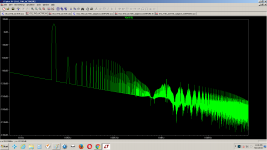
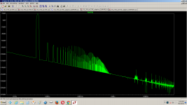
Did an FFT and found that anything above 1Mhz the harmonics are literally cancelled but below there is no effect. Its actually doing the job but all above 1Mhz
Attachments
Last edited:
any comments?used BJT in the output.
Did an FFT and found that anything above 1Mhz the harmonics are literally cancelled but below there is no effect. Its actually doing the job but all above 1Mhz
There is one more problem that im facing building kypton v2 is that one of the LEDs glow for a moment and turn off when I increase the voltage to 50V with 12V being the zener which powers the input stage.
Transistors BC550C beta in the range of 600 and source resistors tested with 100ohms to 33ohms but since the beta is high i suspect an oscillation. so tried to increase the compensation cap in the input stage from 100pf with 270ohm in series to 200pf and even tried less values also but no use why is this happening?
Im more thinking its oscillating so any chance to reduce the oscillation?
Increase the source resistor at the input transistors to 200 or so?
since its input stage there are hardly any parameters to control which I feel.
One LED gets 1.6V and other either gets 0.06V or 0.01V sometimes.
what do you suggest in this case?
There is one more problem that im facing building kypton v2 is that one of the LEDs glow for a moment and turn off when I increase the voltage to 50V with 12V being the zener which powers the input stage.
Transistors BC550C beta in the range of 600 and source resistors tested with 100ohms to 33ohms but since the beta is high i suspect an oscillation. so tried to increase the compensation cap in the input stage from 100pf with 270ohm in series to 200pf and even tried less values also but no use why is this happening?
Im more thinking its oscillating so any chance to reduce the oscillation?
Increase the source resistor at the input transistors to 200 or so?
since its input stage there are hardly any parameters to control which I feel.
One LED gets 1.6V and other either gets 0.06V or 0.01V sometimes.
what do you suggest in this case?
Hi Rhythmsandy, if one of the LEDs in LTP collectors is not glowing, you've got the whole circuit seriously unbalanced, so you should see a significant DC offset at the output. Right?
Also, if you've got no oscilloscope connected to the output, it's rather difficult to see what's going on.
no actual problem is that it glows when the voltage is low and once increased through dimmerstat it turnsoff. I thought if there is any imbalance in source resistor but its not there is a pot which is precisely adjusted accordingly.Hi Rhythmsandy, if one of the LEDs in LTP collectors is not glowing, you've got the whole circuit seriously unbalanced, so you should see a significant DC offset at the output. Right?
Also, if you've got no oscilloscope connected to the output, it's rather difficult to see what's going on.
I have another question reg the volume pot connected at the input. I have input impedance as 22k but used a 50k log pot so the volume is kind of different at different positions like at full volume its like reduced by 50% and at 80% volume its almost full. Do I need to reduce the pot value to 20k or 10k? which is best?
Hi everyone.
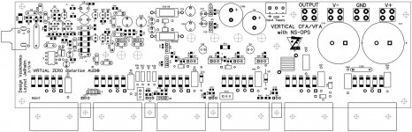
I'm laying out my own 4 pairs OPS board.Do you think that put the output transistors on both side of the PCB (like the image below) will cause thermal inequality ?
Bcs when we put the heatsink vertically the upper part will get hotter thanks to the convection.
Thanks.
I'm laying out my own 4 pairs OPS board.Do you think that put the output transistors on both side of the PCB (like the image below) will cause thermal inequality ?
Bcs when we put the heatsink vertically the upper part will get hotter thanks to the convection.
Thanks.
Yes, the upper row of devices will be attached to a slightly hotter part of the heatsink.
It is usual to offset the two rows downwards to try to equalise the interface temperatures.
The manufacturers give data on how far to move the devices, but you can simulate it with heastink simulation software.
The bottom row at ~ 25% up and the top row ~60% up gives near equality.
You also need to space them laterally to obtain equality of interface temperatures.
The middle devices of those closely spaced colums will run much hotter and thus have higher hFE and lower Vbe, if BJTs, i.e. they will draw more current than their outer neigbours and run even hotter as a result.
This is where R.Cordell's temperature stability guidance come to help.
But if you develop the layout - it makes sense to consider this kind of arrangement.
Note - on a bigger powerful one (left picture) transistors are "shuffled" in a way:
pnp - npn - pnp - npn - pnp - npn
Note - on a bigger powerful one (left picture) transistors are "shuffled" in a way:
pnp - npn - pnp - npn - pnp - npn
Attachments
Thanks for the helpful info, Andrew 🙂
So which way is better ?
I always like the looking of the board with dual sided transistor arrangement, but for the sake of thermal performance, should i follow Valery's board : put all of them on one side ?
Ps : Nice layout Valery.How is the performance compare to the dual sided MT-200 NS-OPS board ?
- Home
- Amplifiers
- Solid State
- Slewmaster - CFA vs. VFA "Rumble"