This is true....if there is oxigen can touch them. But it's not possible inside the paste.Copper and aluminum aren't a good mix when conducting electricity. Many houses have burned down from this.
Sajti
The main idea behind my construction is not the heatsink acting as conductor for the power supply, but to avoid the insulator between the output transistor and the heatsink. I can dissipate much more power on same heatsink, with this solution.
Sajti
Sajti
Attachments
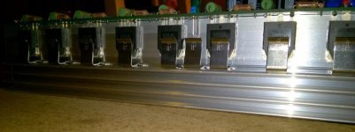
The main idea behind my construction is not the heatsink acting as conductor for the power supply, but to avoid the insulator between the output transistor and the heatsink. I can dissipate much more power on same heatsink, with this solution.
Sajti
How much more power? Have you measured them to failure?
How much more power? Have you measured them to failure?
Not yet, it's under development. The planned output is 600W/4ohms...
It's not so easy to predict, it's depending by the thermal resistance of the heatsink. But my calculation shows, that I can let the temperature up to 95C without insulator, and 70C with insulator.
What kind of failure You mean?
Sajti
Last edited:
"Golden amp"
Here is where my subconscious mind came up with the "slewmaster" -
http://www.diyaudio.com/forums/solid-state/28683-pavel-dudeks-upupa-epops-amplifiers-4.html
Ahh ! the golden amp !
First thing I saw in 2008.
He uses gold plated 12mm copper bars (below) , screws his mosfets directly
to them. He then uses teflon tubing and highly torques the bars to his
heatsink with insulated washers.
This still gives me a new idea for the closely spaced slewmaster OPS.
Just a copper plate under each row of outputs insulated from the heatsink
would turn all 5 into one equalized thermal unit.
I still want mine on the new V2.0 PCB , but the above would make a V1.x
board ideal.
ps - it took me a longggggg time to find that thread !
OS
Attachments
How much more power? Have you measured them to failure?
I've calculated over a 40% increase in power with 5U 300mm heatsink using
a version 2.0 slewmaster and spreading the thermals out.
Add a copper heat spreader strip under the rows of outputs or using
the MT-200's with their bigger slug , add another >10%.
That is just a conservative thermal derating curve estimate. Power over
time and in warmer environments would also greatly increase.
CPU HS's with a copper slug easily run 10C cooler , adding a 1/8" copper
bar to (under) the row of outputs gives an instant 10-20%.
OS
ps - it took me a longggggg time to find that thread !
Ah! Your computer skill is way below your electronics skill! 😛
If only for the picture, I can search locally in my hard disk. But instead of using gold, I prefer using better capacitors there 😀
I've calculated over a 40% increase in power with 5U 300mm heatsink using
a version 2.0 slewmaster and spreading the thermals out.
Add a copper heat spreader strip under the rows of outputs or using
the MT-200's with their bigger slug , add another >10%.
That is just a conservative thermal derating curve estimate. Power over
time and in warmer environments would also greatly increase.
CPU HS's with a copper slug easily run 10C cooler , adding a 1/8" copper
bar to (under) the row of outputs gives an instant 10-20%.
OS
Add some silent running fans, You can reach 20% of the original thermal resistance of the heatsink, and You can dissipate 5times the power comparing to concvection cooling.
Sajti
Ah! Your computer skill is way below your electronics skill! 😛
If only for the picture, I can search locally in my hard disk. But instead of using gold, I prefer using better capacitors there 😀
No , my mind is "soft" .... I forgot who ? (Upupa Epops).
OS
Add some silent running fans, You can reach 20% of the original thermal resistance of the heatsink, and You can dissipate 5times the power comparing to concvection cooling.
Sajti
First there is the 6-7mm chip inside the output. In the case of the NJW's
a 20mm square copper spreader. Then that 20mm slug dissipates through
an insulator to the aluminum.
Nothing we can do about that first interface inside the device.
the 20mm output slug , if interfaced to a much larger copper bar ...
has a much larger interface with the aluminum.
This is the "ploy" of the best CPU heatsinks. A 35mm round copper
bar "wrapped" by the finned aluminum heatsink - increases the
CPU's heat spreader surface many times (at the aluminum interface).
OS
Maybe I was not careful enough. Adding fan, let You to dissipate 5times the power with the same heatsink. But not with the same amplifier. To reach it, You have to add more output devices to the same heatsink.
Anyway this amp is just a prototype, and I use cheap output devices. The final version will use Sankens, even not MT200 version.
Sajti
Pavel has always been one of the most gracious people over on the Blowtorch thread, he always helps when I have a question and gives me easily understood concepts and references to documents to take things to a higher level. A very well informed poster here on this site.
First there is the 6-7mm chip inside the output. In the case of the NJW's
a 20mm square copper spreader. Then that 20mm slug dissipates through
an insulator to the aluminum.
OS
There is easy way to increase the copper spreader. Just add some more output devices. They are quite cheap, and they are containing the copper too...
Sajti
Looking at the pictures just posted by carcass my question is does the transistor radiate equal heat on both sides of the package or is the internal die closer to the side we normally mount them on? If it is equal then those copper plates make a lot of sense for increasing the radiated surface ares to lower the die temperatures. I guess those little copper plates could end up being a secondary small finned heat sink.
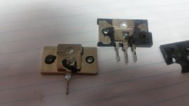
The die is mounted on the metal tab on the rear of the transistor. Here's a picture of some MT-200s I exploded.
Attachments
Thanks JW,
Then there is a major difference in the flow path of the heat. No real advantage then besides adding some even clamping pressure on the radiating surface side against the heat sink.
Then there is a major difference in the flow path of the heat. No real advantage then besides adding some even clamping pressure on the radiating surface side against the heat sink.
Thanks JW,
Then there is a major difference in the flow path of the heat. No real advantage then besides adding some even clamping pressure on the radiating surface side against the heat sink.
I'm wondering why they don't mount the die right on the heat spreader. That extra connection between the plates seems unnecessary.
Just looking at the destroyed device I have more questions than answers about the construction and why they do what they are doing. The actual semi-conductor material is really small in respect to the package. Then you have the stepped section at the top of the part and is that an internal sink built into the device? Then why is there that counter sink hole in that top section? I imagine this all has to do with manufacturing methods, cost, and the determination of the SOA of the device given a minimum amount of heat transfer. As I say I am only conjecturing based on what I can see of the actual physical construction here.
TO-3P = .81C/W
TO-264 = .7C/W
MT-200 = .62C/W
That is , junction to case thermal resistance.
Most likely why a MT-200 has higher SOA.
From TO-3P to MT , doubling the slug area gives 50% more wattage.
MT-200 dies don't look bigger than TO-3P's.
But , Sanken's ring emitter semi might also be more robust.
OS
TO-264 = .7C/W
MT-200 = .62C/W
That is , junction to case thermal resistance.
Most likely why a MT-200 has higher SOA.
From TO-3P to MT , doubling the slug area gives 50% more wattage.
MT-200 dies don't look bigger than TO-3P's.
But , Sanken's ring emitter semi might also be more robust.
OS
TO-3P = .81C/W
TO-264 = .7C/W
MT-200 = .62C/W
OS
Where did You get this values?
Sajti
Just looking at the destroyed device I have more questions than answers about the construction and why they do what they are doing. The actual semi-conductor material is really small in respect to the package. Then you have the stepped section at the top of the part and is that an internal sink built into the device? Then why is there that counter sink hole in that top section? I imagine this all has to do with manufacturing methods, cost, and the determination of the SOA of the device given a minimum amount of heat transfer. As I say I am only conjecturing based on what I can see of the actual physical construction here.
The countersunk hole is normally full of the material bonding the two parts. It ripped out with the epoxy. I think the inner tab is the same as would normally be used for a TO-247 device.
- Home
- Amplifiers
- Solid State
- Slewmaster - CFA vs. VFA "Rumble"