That's always an option but there's more of a chance of lead breakage that way. OS mentioned it was possibly a source of oscillation when I was having problems a while back.
I see you used the vertical design for your output inductor. I like the look of them but mine always end up getting bent. The wood filler is a good idea while working on the amp. I might try that in the future.
The wood core sit in place and isn't just for working on PCB...
The wood core sit in place and isn't just for working on PCB...
That would make them even harder to damage. Does the wood have any effect on the inductors operation? I know there's supposed to be nothing inside an air core inductor but I'm curious if wood or plastic would have any effect on it?
That would make them even harder to damage. Does the wood have any effect on the inductors operation? I know there's supposed to be nothing inside an air core inductor but I'm curious if wood or plastic would have any effect on it?
To have an effect core has to be magnetic matérial. The wood core idea is taken from copperband speaker inductors.
The wood core is equivalent to air in inductance. I've done that for years on speaker inductors. Leave the wood inside for mounting purposes.
Placing the 22uf near to OP collector is quite difficult in respect of curent flow. Will it an issue to put then a little less narrow collector leg, reduce the number of them (3->2) may be growing their value from 22 to 33 or 47uf?
Placing the 22uf near to OP collector is quite difficult in respect of curent flow. Will it an issue to put then a little less narrow collector leg, reduce the number of them (3->2) may be growing their value from 22 to 33 or 47uf?
I put 100uF in mine. This is one time the axial version RE resistor works out better.
Attachments
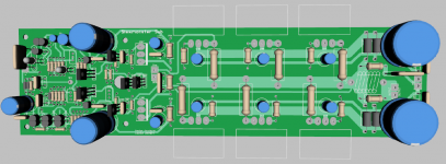

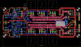
Following Jason advices you can find under PCB rework. Board is 24mm longer as my first version
Marc
Marc
Attachments

Last edited:
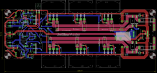
Following Jason advices you can find under PCB rework. Board is 24mm longer as my first version
Marc
The main caps look much better now. If you could squeeze the ground in with the power rails it would be perfect but there's not enough room for that with those RE resistors.
I'm Jeff by the way. Jason does much nicer looking boards than I do.😉
The main caps look much better now. If you could squeeze the ground in with the power rails it would be perfect but there's not enough room for that with those RE resistors.
I'm Jeff by the way. Jason does much nicer looking boards than I do.😉
Sorry for name mistake Jeff. Yes There is not enough room for those ground route with MPC71...but i have a full buckett of them and they are good non inductive resistors...Thank for all advices Jeff.
Marc
Sorry for name mistake Jeff. Yes There is not enough room for those ground route with MPC71...but i have a full buckett of them and they are good non inductive resistors...Thank for all advices Jeff.
Marc
I've seen other designs where the power rail runs on the top side of the board and the ground runs directly below it. The caps are placed through both rails and connected like you would in a plane. I've always been curious if the two rails would cancel each others noise emissions out or if the ground would just pick up hum. In your application that would require 2 oz copper which would really raise the cost though.
Could an overlay of a thin trace with some 12 or 14 ga. solid house wire be doable?I've seen other designs where the power rail runs on the top side of the board and the ground runs directly below it. The caps are placed through both rails and connected like you would in a plane. I've always been curious if the two rails would cancel each others noise emissions out or if the ground would just pick up hum. In your application that would require 2 oz copper which would really raise the cost though.
Could an overlay of a thin trace with some 12 or 14 ga. solid house wire be doable?
Just about every car amp was done like that 20 years ago. It messes up the solder mask appearance though. I'm not sure if the power and ground rails back to back on opposite sides of the board would be good or bad.
I've seen other designs where the power rail runs on the top side of the board and the ground runs directly below it. The caps are placed through both rails and connected like you would in a plane. I've always been curious if the two rails would cancel each others noise emissions out or if the ground would just pick up hum. In your application that would require 2 oz copper which would really raise the cost though.
I've seen a silicon image amp kit PCB with the V+/V- on opposite sides.
Running the rail opposite ground would provide some cancellation of half wave
current pulses for that rail. You would then lose the ability to make a double sided
20A+ Xmax rail ... another trade-off !
But , I have noticed it is the circuit "behind" the initial driver/predriver decoupling
that is sensitive to EMF.
Anything radiated by the typical OPS layout is in "good company" with the
inductor , twisted triplet , and being in close proximity with a trafo (in a
typical chassis layout).
For MT200's or a 5 pair setup .... greater thermal spacing is ideal.
The MT- 200's have a larger heat spreader -- with 3 pair , it tests ideal.
If you were to have 5 of them , that's a LOT of dissipation ! (2300W of
device). Spread this as far apart as possible.
Edit - the accuphase and other "esoteric" high current amps have NO
rail traces. They run a stamped copper bus across the top of the board
soldered at each output collector pad. Sony 5 channel HT receivers do this , as well.
OS
Last edited:
Hi all, i have some questions about latfet slew version. I redrawn layout to be abble to use AFL16N16/ALF16P16 double die version. I suppose doubling die means reworking biasing but i unabble to do it. Could some one advise me. I would use this OPS with +/- 42 or 50Vdc rail. I join you the schematic and the redrawn layout.
Attachments

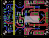
Looks like the ALF16n16w is the same pinout as the Renesas devices so I'm confused as to why a new layout is needed. What am I missing?
Looks like the ALF16n16w is the same pinout as the Renesas devices so I'm confused as to why a new layout is needed. What am I missing?
What you mis is that AFL16x16 is a To264 package as Renesas are To3p so smaller but with same pin pattern. You can see on my layout 2 hole per To264 package=> the second hole is for single die version => similare to To247 package.
Marc
OK so the difference is the mounting hole for the larger device? Seems that could just be drilled into the existing boards. Any other changes?
- Home
- Amplifiers
- Solid State
- SlewMaster Builds