Maybe an updated version of the pcb could include these test points, even simple vias nearby the resistors.
Will you cut the leads after the settings or do you plan to leave them like that?
Vias for the jumer JP1 could be also used for bias measurement when adjusting. (measuring mVolts over 0R1 resistor R15)
I overlooked, it would be probably better, if output caps on the main pcb are used, for C14 to use larger value film cap, 4.7uF/50V or even 10uF/50V that can fit into footprint on the pcb.
...Btw I noticed that you placed 3 pins instead of VR20? That trimm pot is not optional
it is used as a RB for max idle current and RB1-4 are used in parallel connection to VR20 for lower idle current settings.
Hi Borko,
I misunderstood, I thought the trimpot (VR20) was used to get a resistance measurement for the desired bias current, then use a fixed resistor of that value for one of the RB1-4 locations. Then repeat the procedure with different bias current for the other RB locations. When done, remove the trimpot.
But, if VR20 is initially set to 75K for 1.5A bias and is in parallel with SW1, when I flip the dip switch ON to get 1.5A bias a 64k resistor is now in parallel with VR20 dropping the overall resistance to 34K5.
How can 75k and 34K5 both equal 1.5A bias?
I think I’m missing something......
If you planned on using a rotary type switch, one resistor would always be in parallel with VR20, thus keeping resistance in the 26k - 35k range.
The Dip switches are either ON or OFF, there could be a time when all switches are OFF and then the full 75K of VR20 would be seen. Could this situation be catastrophic for the amp?
Maybe the on/off dip switch bank is not ideal?
Hi Vunce, on reading the article, I was also a bit confused on the biasing with the trimpot, fixed resistors and the DIP switch, maybe Borko can explain that all a bit clearer - as it is important.
Also what transistor did you use for T1 (2SA1220 or BD140). Are you going to use the cap bank board and do you have a particular audio grade 10,000uF cap in mind for C13?
Also what transistor did you use for T1 (2SA1220 or BD140). Are you going to use the cap bank board and do you have a particular audio grade 10,000uF cap in mind for C13?
Hi Gary,
I made a Mouser list, look at post #95
Single Ended cfa
I’m going with KSA1220 and Nichi KG for C13.
No external capacitor bank for the initial build, that’s something to play with down the road.
I made a Mouser list, look at post #95
Single Ended cfa
I’m going with KSA1220 and Nichi KG for C13.
No external capacitor bank for the initial build, that’s something to play with down the road.
Ok I obviously didn't write well, update tomorrow...
Thing is, VR20 is always in the circuit and with dip switches off. It says in the article, RB4 NC no connected resistor. So max bias is with only VR20 in circuit, by switching RB1 or RB2 or RB3 ON, you are connecting 160K or 220K or 680K in parallel with the VR20 wich gives lower bias currents then max value adjusted with VR20 only.
I'm using KSA1220 but BD140 could be used, thre are the distortion measurements with different transistors in the thread..
Nichicon KG would be fine.
Of course as said in the article one could use DIP switch OR a rotary switch.
Maybe is DIP sw better option for initial testing.
Cheers 🙂
Maybe is DIP sw better option for initial testing.
Cheers 🙂

Values for "bias resistor" (RB1,2,3,4...) :
0.5A 39K
0.8A 47K
1A 51K
1.2A 56K
1.5A 64K
1.8A 78K
I think I found the confusion about the discrepancy of bias resistor values.
Borko, does the above list give the paralleled final resistance value of VR20 and RB?
Examples:
VR20 75K // RB 160K = 51K
VR20 75k // RB 220K = 56K
I think I found the confusion about the discrepancy of bias resistor values.
Borko, does the above list give the paralleled final resistance value of VR20 and RB?
Examples:
VR20 75K // RB 160K = 51K
VR20 75k // RB 220K = 56K
Yes, that`s it. VR20 is the "main bias resistor" and RB1-4 are connected in parallel (look at schematic) each one giving different, lower bias current...
Yahoo!!
The figures didn’t make sense because I was using this earlier list from post #83.
Ok, I’ll update the RB1-4 resistors in the Mouser parts list.
The figures didn’t make sense because I was using this earlier list from post #83.
Ok, I’ll update the RB1-4 resistors in the Mouser parts list.
Ok, thanks . BTW those RB resistors are ~ values, so not 100% right, when you assemble all, you could use one 100-200K trimmer or pot as variable RB resistor to get exact values. I`m curious will they match. Have you measured hFE of BC556B?
Thanks a lot Borko, with your update and Vunce's questions and your answers, the biasing scheme is well understood now.
Article update 1.2
Some corrections and more data about clipping and mouser part list link (thanks to Vunce):
Some corrections and more data about clipping and mouser part list link (thanks to Vunce):
Attachments
Last edited:
Hi Borko and Vunce, I calculate the value of RB3 (to give a parallel resistance of 64.6K) to be 470k and not 680k. Also for RB4 to give as close as possible to 78K (actually 74.4K) it should be 10 Meg (not 3.9Meg) or leave it open to see the total pot resistance of 75K.
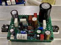

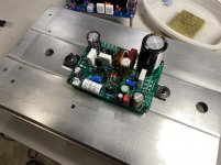
Nice work Vunce, looking very new and shiny. What rail voltage are you going to use - just normal CRC or cap multiplier like SLB I wonder.
- Home
- Amplifiers
- Solid State
- Single Ended CFA