That was a quick repair. Broken 9610s from static or some short then.
What is the DC across R1x pins now? What is the loaded RAW DC now?
Do both sinks warm up? Rail+ became properly adjustable?
What is the DC across R1x pins now? What is the loaded RAW DC now?
Do both sinks warm up? Rail+ became properly adjustable?
Raw DC is now 52 VDC, my Rail + was 29 VDC with R3x at 9.1K. I changed R3x to 16K, all I had that was close, and now the Rail + is 39 VDC.
I'll order the 12K resistors for R3x and the 33 ohm resistors for the LINK.
Once I have them installed with the Rail + at 35 VDC, I'll measure the voltage drop across R1x and post it.
I'll order the 12K resistors for R3x and the 33 ohm resistors for the LINK.
Once I have them installed with the Rail + at 35 VDC, I'll measure the voltage drop across R1x and post it.
Where is TP2 on the PCB? I found TP1 and Rail +, however, I can't find TP2.
TP2 is printed at one side of R4 & R14. Their legs at that side is the probe node.
Drop across R1x has not to do with Rail + level. Must be there regardless.
Rail + may end up other than 35V for good TP reading. Just a starting point.
Especially in MM config, Rail + most usually ends up significantly lower than 35V.
Rail + may end up other than 35V for good TP reading. Just a starting point.
Especially in MM config, Rail + most usually ends up significantly lower than 35V.
I have 1.41V across R1x.
By installing the 16K at R3x, it gives a Rail + of 39V, should I go back to the 9.1K for R3x?
9.1K at R3x gives 29V for Rail +.
By installing the 16K at R3x, it gives a Rail + of 39V, should I go back to the 9.1K for R3x?
9.1K at R3x gives 29V for Rail +.
I found TP2, C1 was blocking my view by casting a shadow where TP2 is.
Is the adjustment for TP1 - TP2 more important (accuracy) than the Rail + measurement?
I stopped because Rail + was 39V, didn't want to burn up anything.
Is the adjustment for TP1 - TP2 more important (accuracy) than the Rail + measurement?
I stopped because Rail + was 39V, didn't want to burn up anything.
1.41V across R1x is fine. Means 94mA CCS. Most usual.
TP reading is your arbiter. Rail + you adjust to achieve that.
For now put two 22k resistors in parallel as R3x or 2.2k in series to 9.1k.
TP reading is your arbiter. Rail + you adjust to achieve that.
For now put two 22k resistors in parallel as R3x or 2.2k in series to 9.1k.
OK. I'll see what values I have, and change R3x accordingly.
Now I understand TP1 - TP2 adjustment, the Rail + voltage adjusts the TP level.
Now I understand TP1 - TP2 adjustment, the Rail + voltage adjusts the TP level.
I have TP1 - TP2 = 3.60vdc
Rail + = 34vdc
I'm going to let it cook for an hour and then do the other board.
I used a 2.2K Vishay RN60 resistor with the 9.1K for R3x.
Rail + = 34vdc
I'm going to let it cook for an hour and then do the other board.
I used a 2.2K Vishay RN60 resistor with the 9.1K for R3x.
The second channel
Voltage drop across R1x = 1.25vdc
Rail + = 37.8vdc
TP1 - TP2 = 5.6 - 6.0vdc
Adjusting VR2x does not seem to make a difference to TP1 - TP2.
Voltage drop across R1x = 1.25vdc
Rail + = 37.8vdc
TP1 - TP2 = 5.6 - 6.0vdc
Adjusting VR2x does not seem to make a difference to TP1 - TP2.
Confirm that the rail+ itself does not adjust also. Compare Vgs between IRF9530s Q6x in the good PSU and in the bad PSU. Maybe it needs replacement in the bad one. As you initially had broken Q1x Mosfets for some reason, you may have one more in another position. Next thing to compare is Vbe voltage of Q4x BC550s. Pins 2-3.
Hello Salas -
I confirmed that the Rail + voltage does not respond to adjustments of VR2x.
Rail + = 32.5vdc
TP1 - TP2 = 6.65vdc
Good Channel Bad channel
Q1x Vgs = 4.30vdc Q1x Vgs = 4.27vdc
Q6x Vgs = 3.60 vdc Q6x Vgs = 3.65vdc
Q4x Vbe = 0.60vdc Q4x Vbe = 0.62vdc
Voltage drop across R1x = 1.41vdc Voltage drop across R1x = 1.27vdc
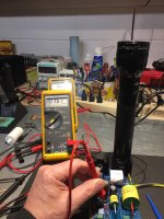
I'm not sure why, if I apply pressure to the heat sink for Q1x, I'm able to adjust TP1 - TP2. The volt meter in the picture shows -3.59vdc, I have the probs reversed. When I apply pressure to the TP2 pad or twist the PCB, the reading changes either to 0.00 or 6.xx vdc and may eventually go back to 3.59 vdc. I've been re-soldering every connection and part on the board with no perfect results, it is better, meaning that I'm measuring 3.60 vdc more than not. I've tried wiggling parts, moving transistors, I even unbolted Q1x from the heat sink.
I'm going to spend time with an ohm meter checking traces.
Could it be a bad capacitor somewhere?
I'm going to spend time with an ohm meter checking traces.
Could it be a bad capacitor somewhere?
Bad cap or a bad joint comes to mind. Did you use ROHS solder? Such alloys need extra heat and don't flow too well. Also inspect for cracks near the plated holes. Especially inspect/redo joints of C8 Q1 Q3 R2 R13. Check if Q1's sink had scratched the solder mask somewhere and closes circuit with some lane that it shouldn't.
I'm using Kester 44 solder from a spool I won in 1971, small desk fan was added just after that. I'll check the pads and areas you recommended first. I'm not positive that pressure/twist of the PCB is the reason for correct voltage at TP1 - TP2. I may make a jig to mount the PCB so I can spin without twist, with a Known Good Channel (KCG), I have a reference to use for voltage checks.
Hello Salas -
I inspected the PCB at C8, Q1, Q3, R2, and R13 as per your suggestion. NDF
I have had the "bad" channel operating off the power supply for the past week.
Symptoms are not as severe, seems like it was getting better, except when I would touch the heat sinks for Q1x and Q6x, then the TP1 - TP2 voltage would vary by +- 1 vdc.
I received my order from Mouser with the 33 ohm resistors for the LINK positions in the power supply. I removed the jumpers and soldered the 33 ohm resistors in place.
The unloaded power supply is now 49.5vdc for each channel.
I hooked up the "bad" channel and I now have the following:
RAIL + = 33.75 vdc
TP1 - TP2 = 3.60 vdc
Dead stable, easy to adjust, no more variations of TP1 - TP2 voltages whenever I touch heat sinks, PCB or anything else!
I'll continue to test the rest of this week, however, everything looks great now!
Thank you again for all your help, I'll post if anything changes.
Time to start drilling the holes in the enclosure for the preamp section.
- Home
- Source & Line
- Analogue Source
- Simplistic NJFET RIAA