Hi Salas,
with circuit off
Q4 VBE measures into MOhm region
Q5 = 500R VBE, trimmer is okay.
I removed the replacement Q3 and placed it in a simple tester, and it was blown. Not sure why.
I tested the original Q3 that was in the circuit when the original short occurred and it shows only 0.2VGS in circuit. When removed and placed in the tester it has the following readings:
Vt = 3.29V
Cg=2.71nF
Rds=1R
DS=570mV
I removed D3 but didn’t manage to test it because it broke while I was taking it out.
D1 and D2 both test okay.
Both DN2540s have been checked in the tester and against new devices; they all show around the same values in the tester.
I’m using a dummy load that only draws 14ma from the output.
I guess Q3 might be the problem?
Q3 could have even blown from static discharge when handled or when soldering with non earthed iron. Mosfets are notorious for having a thin sensitive gate oxide layer. Yes it can be the problem, as much as any other semiconductor in this circuit.
I'm thinking to buy couple of pcb from teabag... I already have 8pcs K117GR5F (hoping they are not fake) instead of the specified 2SK117GR... may I use them or? I'm not able to understand if there are differences between the two codes... I can only find a very old data sheet from Toshiba that is absolutely not clear
You can use one in SSHV2 if genuine. 5F is a production code among others. It is always there after the main code. Better show us a close up photo to advise you for fake clues if any.
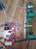
I have update the resistors today,change from 68K to 56K and no other change,the voltage can support lower to 80V and output noise about 1.1mv,I guess it should be adjusted for the main filter
yes,but the noise still a litter bitter high.I think i need to finger out how to reduce the noise.
yes,it is hum phono noise.it is base on the MM model and add SUT before it.
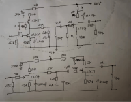
I have tried two version of schematic, one is your version and only change some resistors and JFET and another one is also base your version cascade mode and change the jfet to k79.attached please find for two version of schematic.
I have tried two version of schematic, one is your version and only change some resistors and JFET and another one is also base your version cascade mode and change the jfet to k79.attached please find for two version of schematic.
Attachments
Last edited:
Hum in prototype phonos can be due to many reasons. Layout, wiring, lack of shielding, lack of chassis, ground loop, PSU ripple if there's also buzz sound. Needing to investigate all those aspects.
By the way, that top FET looks more like a CCS? Would be gate biased with a voltage divider and output from the drain as typical cascode?
By the way, that top FET looks more like a CCS? Would be gate biased with a voltage divider and output from the drain as typical cascode?
Nice, also use top layer ground shield next time. To be more secure about noises especially before installed in a grounded chassis.
next plan is use chassis firstly also will rerouting the ground. I will follow it and check moreHum in prototype phonos can be due to many reasons. Layout, wiring, lack of shielding, lack of chassis, ground loop, PSU ripple if there's also buzz sound. Needing to investigate all those aspects.
By the way, that top FET looks more like a CCS? Would be gate biased with a voltage divider and output from the drain as typical cascode?
You are right.that is my fault to draw the schematic.the first stage output from the top K79 Drain pin.
- Home
- Amplifiers
- Power Supplies
- Simplistic mosFET HV Shunt Regs