Pop corn
Hi all,
So, did the mod with IRFBE30 as Q3 and KSA1156 for Q5 and Q6.
I went with a big 1.5C/W sink on Q3, I'll think later on for room to fit it in.
Everything went OK, first replacing parts one by one on a running original device at 350Vout. Then I increased by 50V steps Vin keeping 25V on the CCS. Went up to 600V Vout without trouble nor arcing. Was relieved.
Next switch off/on, 3 resistors from the input PI filter caught on fire...
I certainly overlooked euro21 advise, didn't yet changed Q1 for higher voltage one. Bought IXTP05N100 as Mouser was running short but did not replace it for the first run...
Well, silly me, Q1, Q3, Q5, Q6 are shorted, as well 2 zeners. The third one measured a bit different than a new one, so replaced it along with Q2.
I understood post burning that euro21 free advise was for the internal transients of the Shunt regulation. With the big 10uF capacitor, Vout needs 2 or 3 seconds to build up, much slower than Vin. At that time the CCS sees a bigger voltage drop that DN2540 cannot stand, so Q1 got killed, shorted.
Don't know why Q5 and Q6 followed, will try to spice that.
I bought some 2SK880 as a replacement for 2SK117 but didn't realized how small these were till I opened the parcell.
It's quite a bit delicate to use.

Does any of you know a good source on the bay to get genuine 2SK117GR ?
Thank you
Laurent
Hi all,
So, did the mod with IRFBE30 as Q3 and KSA1156 for Q5 and Q6.
I went with a big 1.5C/W sink on Q3, I'll think later on for room to fit it in.
Everything went OK, first replacing parts one by one on a running original device at 350Vout. Then I increased by 50V steps Vin keeping 25V on the CCS. Went up to 600V Vout without trouble nor arcing. Was relieved.
Next switch off/on, 3 resistors from the input PI filter caught on fire...
I certainly overlooked euro21 advise, didn't yet changed Q1 for higher voltage one. Bought IXTP05N100 as Mouser was running short but did not replace it for the first run...
Well, silly me, Q1, Q3, Q5, Q6 are shorted, as well 2 zeners. The third one measured a bit different than a new one, so replaced it along with Q2.
I understood post burning that euro21 free advise was for the internal transients of the Shunt regulation. With the big 10uF capacitor, Vout needs 2 or 3 seconds to build up, much slower than Vin. At that time the CCS sees a bigger voltage drop that DN2540 cannot stand, so Q1 got killed, shorted.
Don't know why Q5 and Q6 followed, will try to spice that.
I bought some 2SK880 as a replacement for 2SK117 but didn't realized how small these were till I opened the parcell.
It's quite a bit delicate to use.
Does any of you know a good source on the bay to get genuine 2SK117GR ?
Thank you
Laurent
Maybe a SOT23 to DIP adapter?
BOB-00717 SparkFun Electronics | Prototyping Products | DigiKey
P.S. Use fuses when testing. Most probable is you need a higher voltage DMOS as you said but maybe a smaller value Vref filter cap also.
BOB-00717 SparkFun Electronics | Prototyping Products | DigiKey
P.S. Use fuses when testing. Most probable is you need a higher voltage DMOS as you said but maybe a smaller value Vref filter cap also.
Maybe a SOT23 to DIP adapter?
BOB-00717 SparkFun Electronics | Prototyping Products | DigiKey
P.S. Use fuses when testing. Most probable is you need a higher voltage DMOS as you said but maybe a smaller value Vref filter cap also.
Thank you Salas, both good ideas.
Found that at mouser : SC70-6 SchmartBoard
And yes I'll also decrease C2, lets say 1u. That will probably increase the noise floor, but that's still far above my actual supplies.
One point I noticed, voltage sets up 6 to 7 Volts below the setting and it takes half an hour to stabilize. I suppose that thermal drift is due to Q3 Temperature Coefficient. The big sink is may be the reason why it takes that long.
A fuse would have maybe avoided killing that much devices, that's probably a better use than having them sitting in the drawers...
Laurent
Last edited:
They are all located near together. Just the thermal radiation on the tiny JFET could do that. It will hopefully improve when on the adapter. Its a very high Vo you use also so see it as 1% Vo thermal settling. Keep in mind that the reg can even work without Q6 if you mod it so to have just R11 between Q5's B-E. Removing Q6 and using a jumper between its D-S pads should achieve that. Make sure it does not touch the gate pad that has a trace shorting across. Then your Vref current will be governed by Q5's VBE/R11(trimmer) only. Less thermals in the system, and bit worse spec.
And yes I'll also decrease C2, lets say 1u. That will probably increase the noise floor, but that's still far above my actual supplies.
Laurent
It will but your I to V Norton type ref is already increased to 200K thus easier to filter than the standard one. 1uF will be somewhat more effective than in the standard reg in other words. Start testing with low uF anyway. Later if you fancy new pyrotechnics you may try find your max acceptable in this 600V mod. 🙂
1uF will be somewhat more effective than in the standard reg in other words. Start testing with low uF anyway. Later if you fancy new pyrotechnics you may try find your max acceptable in this 600V mod. 🙂
I can start at 0.22uF. I like having 4 octaves headroom at cut frequency on audio filtering. So 0.68uF would be optimal if raising time is fast enough to avoid fireworks.
They are all located near together. Just the thermal radiation on the tiny JFET could do that. It will hopefully improve when on the adapter.
That was with K117 FET. Hope it will not worsen too much with the tiny one.
May I try to attach it to the BJT next to it, in order to fastly reach the stable point ?
Its a very high Vo you use also so see it as 1% Vo thermal settling. Keep in mind that the reg can even work without Q6 if you mod it so to have just R11 between Q5's B-E. Removing Q6 and using a jumper between its D-S pads should achieve that. Make sure it does not touch the gate pad that has a trace shorting across. Then your Vref current will be governed by Q5's VBE/R11(trimmer) only. Less thermals in the system, and bit worse spec.
In the tube power amp I build there's 2 PSUs +350V / -550V that feeds the driver stage which has a direct connection to the power stage. If both PSUs present a similar voltage offset and setting time, that could be OK, even having the negative one faster could do it. I'll keep that possibility in mind, might be helpfull.
With the tiny it could take even longer or not. If you will just blow over it you will see. Its the LED that does some counter thermal and its near. Maybe the BJT will heat it to a point that its IDSS gets higher and longer to settle keep drifting, I don't know. Try it. Or a plastic or paper little house to enclose it and insulate it from surrounding temp delta better? Like a greenhouse for a solo JFET vegetable 🙂
With the tiny it could take even longer or not. If you will just blow over it you will see. Its the LED that does some counter thermal and its near. Maybe the BJT will heat it to a point that its IDSS gets higher and longer to settle keep drifting, I don't know. Try it. Or a plastic or paper little house to enclose it and insulate it from surrounding temp delta better? Like a greenhouse for a solo JFET vegetable 🙂
Thank you Salas, time to plug it in.
Laurent
Well, some good news and some others...
When I ordered the IXTP05N100P I did not pay attention that there was a "D" missing at the end, so I received enhancement MOSFET instead of depletion ones : The PSU is dead silent, but at least it did'nt brake anything.
I do have a small overshoot on the Vin supply due to the LC filter, about 20v. I spiced the start and it looks that 0.47uF would be optimal to keep VDS below 200V. So I put back a DN2540 at Q1 location and changed C2 for 0.22uF. Went up step by step to the desired input voltage at 575V and Q1 VDS just went over 100v every time I switched on.
I finally let a 0.47uF in, measured with a DMM set at 1ms catch, VDS remained around 180V max. It looks to be a good margin.
One last trouble, I cannot reach the desired voltage. R11 trimer at min, output voltage topped 20V below my target. I suppose it's due to the 2SK880 version, it has a "Y" suffix, so IDSS is probably too low.
While it's a good thing to increase my stock of unused spares, I should definitely pay more attention to these little alphabetic details.
2SK117GR are on order from the bay, HK source certified as genuine Toshiba...
2SK880GR on order to, along with the SC-70 adapters and finally a set of IXTP01N100D to replace Q1 in case of need.
That should be OK for further testing.
Salas, a question please, if finally R12//R11 is set too close to zero ohm, should I increase R9 & R10 or would it be a too big change to go with a BL FET version ?
Laurent
Much more methodical testing this time. Well done 😉Well, some good news and some others...
When I ordered the IXTP05N100P I did not pay attention that there was a "D" missing at the end, so I received enhancement MOSFET instead of depletion ones : The PSU is dead silent, but at least it did'nt brake anything.
I do have a small overshoot on the Vin supply due to the LC filter, about 20v. I spiced the start and it looks that 0.47uF would be optimal to keep VDS below 200V. So I put back a DN2540 at Q1 location and changed C2 for 0.22uF. Went up step by step to the desired input voltage at 575V and Q1 VDS just went over 100v every time I switched on.
I finally let a 0.47uF in, measured with a DMM set at 1ms catch, VDS remained around 180V max. It looks to be a good margin.
One last trouble, I cannot reach the desired voltage. R11 trimer at min, output voltage topped 20V below my target. I suppose it's due to the 2SK880 version, it has a "Y" suffix, so IDSS is probably too low.
While it's a good thing to increase my stock of unused spares, I should definitely pay more attention to these little alphabetic details.
2SK117GR are on order from the bay, HK source certified as genuine Toshiba...
2SK880GR on order to, along with the SC-70 adapters and finally a set of IXTP01N100D to replace Q1 in case of need.
That should be OK for further testing.
Salas, a question please, if finally R12//R11 is set too close to zero ohm, should I increase R9 & R10 or would it be a too big change to go with a BL FET version ?
Laurent
What do you mean "dead silent" when with a wrong mode Q1? Meaning it does not output Volt anything I would suppose.
LC filter can be damped further with some series power resistor to L. But 20V overshoot is not terrible either.
Yes, insufficient Y type IDSS much probably. That makes you trim R11 all the way down but still on the edge of target Vout. Even that can be addressed with higher value R9-R10 in a case of no other Q6 grade option is in hand.
BL has the more VGS (OFF) of all three grades and could be more prone to drift but not much. In your 600V output special case maybe noticeable. The less VGS (OFF) the more Q6 impedance under little VDS as used in this circuitry position. Although Y that has the less VGS (OFF) it can give very little IDSS thus longer C2 charge up also. Not good when wanting higher C2.
Post a close up picture of your new K117 before installing it. We usually can tell a genuine by print, shape, legs.
Thank you, the method was almost the same but the focus was on a different part. A fuse was also there watching, so every bit kept on the track. 🙂Much more methodical testing this time. Well done 😉
Exactly !What do you mean "dead silent" when with a wrong mode Q1? Meaning it does not output Volt anything I would suppose.
In fact it's a LCRC filter. The 20V are after the final stage and yes, 3% overshoot is fully acceptable.LC filter can be damped further with some series power resistor to L. But 20V overshoot is not terrible either.
I'm not used to manipulate these parameters and their relations. What I think I understand so far is that the higher GM --> the higher IDSS --> the lower VGS(OFF). So I would believe that due to low IDSS/high VGS(OFF) I need a low gate/source resistor to get the righ DS current. This low resistor decreases the I/V conversion that drives the gate and associated with a low GM lowers the AC impedance of the FET which is not a good thing for a current source.BL has the more VGS (OFF) of all three grades and could be more prone to drift but not much. In your 600V output special case maybe noticeable. The less VGS (OFF) the more Q6 impedance under little VDS as used in this circuitry position. Although Y that has the less VGS (OFF) it can give very little IDSS thus longer C2 charge up also. Not good when wanting higher C2.
Consequently going the opposite, higher GM, resistor, IDSS would give a bigger impedance.
There's certainly something I don't understand yet in this voltage reference, thinking too much with tubes in mind.
I'll do it, thanks.Post a close up picture of your new K117 before installing it. We usually can tell a genuine by print, shape, legs.
Laurent
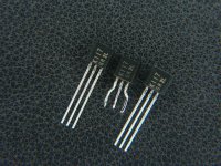
FETs arrived today.
If they are fakes, it's a good copy.
The middle one is from the latest fireworks on HV supply. Marking color is darker yellow/brown, maybe due to heat or dirty fingers.
New ones looks to be laser etched. For the legs I cannot say.
Laurent
If they are fakes, it's a good copy.
The middle one is from the latest fireworks on HV supply. Marking color is darker yellow/brown, maybe due to heat or dirty fingers.
New ones looks to be laser etched. For the legs I cannot say.
Laurent
Attachments
I made also some mechanical controls :
Molding traces are rigorously the same, as well as package mechanical dimensions.
Molding traces are rigorously the same, as well as package mechanical dimensions.
I'm not used to manipulate these parameters and their relations. What I think I understand so far is that the higher GM --> the higher IDSS --> the lower VGS(OFF). So I would believe that due to low IDSS/high VGS(OFF) I need a low gate/source resistor to get the righ DS current. This low resistor decreases the I/V conversion that drives the gate and associated with a low GM lowers the AC impedance of the FET which is not a good thing for a current source.
Consequently going the opposite, higher GM, resistor, IDSS would give a bigger impedance.
There's certainly something I don't understand yet in this voltage reference, thinking too much with tubes in mind.
Laurent
Look at this chart I clipped from the K117 datasheet
Attachments
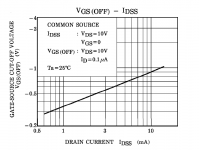
Look at this chart I clipped from the K117 datasheet
Yes, "the higher IDSS --> the lower VGS(OFF)".
And this also : "the higher GM --> the higher IDSS"

So am I wrong if for a given current the polarization resistor is better bigger than too small as a first approach, maybe with the bandwidth limit due to the gate capacity ?
Anyway, I just need to revert to a GR FET and all should be OK. I don't want to rework too much a stable design and finish with an oscillation prone PSU.
Thank you for your great work and help Salas.
Laurent
The higher the IDSS in a certain type's range the higher its VGS(OFF) as an absolute number. Think in terms of power tubes. When you got a tube that produces more mA at a certain voltage bias than its next same tube, don't you need more negative grid voltage to completely shut it off than its neighbor? That's higher VGS(OFF).
VGS(OFF) as an absolute number....That's higher VGS(OFF).
OK, got your point.That was a question of convention. When talking about lower VGS(OFF), I was thinking more negative, not absolute value.
There's a point I have difficulties to express, due to the lack of vocabulary or knowledge. Here it is a different way, facts speaks better than minded projections.
[I installed the new FET, I can now adjust to the desired 550V.
 ]
]There's a few volts variations of Vin, completely random, not much I can do about it, that's also why I need a regulated PSU.
This translate into 50 to 100mV variations on Vout, at low freq and obviuously related.
I do understand that having lowered C2 is part of the behaviour but :
R11//R12 set at 17 Ohm, Q6 VGS is only -46mV, VDS at 0.46V. 2.7mA thru Q6, R9, R10.
I do think that the reference regulation might be poor. It would need a higher polarization resistance. I may be wrong.

The solutions I forecast if any good, from "at hand" to "wait one or two weeks" :
- Increase R9, R10. 150K or 180k .This will lower FET current respectively to 1.8mA and 1.5mA.
- Sort out the FETs, hoping I can get a higher Gm/IDSS.
- Switch to a BL FET.
Don't know the pros and cons neither the side effects, may be just try and see...
Thermal drift improved with the new FET. While amplitude is about the same, it gets stabilized in just 5 minutes, 6 times faster ! And blowing with a BIC tube on the FET brings a immediate drop of 3 volts ! That's the one that does the drift.
Reducing FET current might improve the amplitude to.
Laurent
- Home
- Amplifiers
- Power Supplies
- Simplistic mosFET HV Shunt Regs