Is it like VLF cycling that variation? Or it has broader noise too? Because you can't use high C2, also try that Vbe/R instead of Q6 trick I described to you before.
Hello Salas,
Yes that's low speed variations but there's no evidence of cycling, it looks random. It's on the 230VAC house supply, a few volts, despite transformer is not very far away. There's no HF noise.
In simulation, going from 17 Ohm to a few hundred gives 10db more attenuation.
Hello,
I changed R9,R10 @180K. While Vout was set at 280V, there was random oscillations, 400KHz about 200mV, they went on and off just at the limit. As soon as I increase Vout, they disappeared completely. I'll revert to 150KOhm.
Right now at 550Vout, Fet source resistance is set to 100 Ohm, 6 times more than before. This had no significant effect to solve sensitivity to Vin disturbances.
I received the 1KV depletion Mosfet, so I'll replace Q1 and go back to 10uF C2. Should do the job for a more stable Vout.
I received the 1KV depletion Mosfet, so I'll replace Q1 and go back to 10uF C2. Should do the job for a more stable Vout.
Hi Salas,
Back to original C2 value is OK, works as should do. It needs higher voltage Q1 as this one sees the full voltage at startup. IXTP01N100D right now. Much stable and no more parts popping up.
Noticed that the feedback is highly reactive, connection of a DMM on output makes the voltage drop by a few to several tens on the modded version. The original PSU does the same but max ten volts drop.
The DMM with the bigger effect is 1 meg/50pF input, the second one at 10meg has less effect.
My understanding is that the sharp raising edge of the small current induced by the DMM connection goes beyond the bandwidth of the feedback loop, maybe the time constant with Q3 input capacitor is too high.
Was a bit reluctant to plug it to the tube stage, but I suppose that as long as there's no wrong contact nor RF that should be OK.
Maybe simply put a small cap on output.
Try two wire mode to avoid inductance in the sense loop. The modded seems to have eaten enough phase margin. Maybe smaller R7 too along some revision of the output termination as you say.
Try two wire mode to avoid inductance in the sense loop. The modded seems to have eaten enough phase margin. Maybe smaller R7 too along some revision of the output termination as you say.
I was already in 2 wires mode.
The CCS is working well, no change on the current when the voltage drops. Only the shunt is involved. 1uF on the output did not change much. You're right, I'll play with R7. Maybe short it as a first try.
Maybe smaller R7 too
Thank you Salas, that did it. I went 22 first, better but still picky. Then shorted it, and it's much stable, not far from the non modded. 20/30 volts drop where the second one drops 10. I'll keep an eye on it and keep searching for a better Q3. But it's good enough I think to put it in the amp.
Is there a way/has anyone tried building a less current overhead hungry version for smaller loads, for example with LND150 or such as CCS?
I may be wrong, but it's not CCS that limiting the min current, it is the shunt MOSFET that should work in certain area.Is there a way/has anyone tried building a less current overhead hungry version for smaller loads, for example with LND150 or such as CCS?
I may be wrong, but it's not CCS that limiting the min current, it is the shunt MOSFET that should work in certain area.
Ok thanks for the enlightenment. I thought the shunt mainly needed voltage overhead, but yes, it might be so.
I need a low z stable voltage circuit feeding pentode G2. Sometimes they need only some 200 microamps (like EF86) and flushing 20 mA on that is kind of wasteful. A superstable low z floating voltage source on g2 to cathode is very beneficial.
I need +/-300vdc and will use the attached setup as below.
The only transformer I have has one secondary winding of 646Vac with a center tap (@ 323Vac). Can I use my transformer or do I need two separate secondary winding's (of 323Vac) as per the attached cct diagram?
thanks
The only transformer I have has one secondary winding of 646Vac with a center tap (@ 323Vac). Can I use my transformer or do I need two separate secondary winding's (of 323Vac) as per the attached cct diagram?
thanks
Possibly in p2p for one, not on the positive board, but I haven't looked into it because I prefer this scheme, which is anti ground loop also:
Attachments
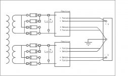
Your diagram shows a dual secondary.
If you want to use two positive regulators you need dual rectifiers and dual secondaries.
you cannot use a centre tapped secondary where a dual secondary feeds into dual rectifiers.The only transformer I have has one secondary winding of 646Vac with a center tap (@ 323Vac)
If you want to use two positive regulators you need dual rectifiers and dual secondaries.
Hi,
I'm running two SSHV2 regulators for 350V DC and 17+20mA overhead per one channel. Hovewer I've noticed that R11 multiturn resistor is very sensitive in the output voltage settings. Looking in the schematics it is in parrarell with R12 (470 ohm) resistor. Maybe I should replace R12 resistor with different one to have more precise tuning?
I've measured resistance of parallel connected R11 and R12 and there are 11,2 ohm and 10,4 for each channel. Please recommend me new R12 value for more precise 350Vseting.
TIA
You could drop 90% of your voltage over the fixed low tempco resistor.
The other 10% could be across the variable resistor. Double the value that gives the 10%. To allow the VR to move around thw half value setting.
eg. you have 350Vref
320Vdrop across 100k gives a current of 3.2mA and a Pdiss of ~1W (use >3W)
The 3.2mA and 20% of 350V gives you the required variable resistance of 70V/0.0032A = 22k, use a 20k VR.
A 20k VR of 500mW max Pdiss has a maximum current of only 5mA.
For this I would increase the 100k to drop nearer 95% and drop the VR to 10k.
Consider what current passes down the Vref string. How much can it be varied?
Thank you Andrew.Consider what current passes down the Vref string. How much can it be varied?
Unfortunately I don't know how a current can be varied. All I know is that one channel (for one SSHV2) consume 17mA and set SSHV2 as 17+20mA
I've measured resistance over parallel connected R11 and 12 (as in the schematisc) and is about 12,5ohm.
Attachments
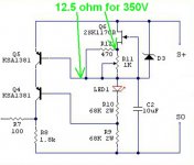
The Vref string is made up with R9 68k, R10 68k, LED1
the Vdrop across that string sets your output voltage because Vout = Vref+Vbeq5
If you vary the current through a resistor you change the vdrop.
Learn how your circuit works before you try to redesign it.
the Vdrop across that string sets your output voltage because Vout = Vref+Vbeq5
If you vary the current through a resistor you change the vdrop.
Learn how your circuit works before you try to redesign it.
Let me "translate" Andrew. The output voltage is defined by the current from the current source Q6R11R12 (which can be changed by R11||R12) and the R9+R10 (through which the current flows and the resulting voltage drop almost = the output voltage). You measured the R11||R12 rather low, it means that you are approaching the high current margin of the current source. You can lower the values of both R12 and R11 certainly, but it will help only partially. So it is better to increase the values of R9 and R10 and stay near the "designed" current - in such case you'll have smooth changing and less heating of Q6.
I believe I've seen this suggestion somewhere in the manual.
I believe I've seen this suggestion somewhere in the manual.
Thank you poty and Andrew
Do you think that 82k/2W (R9,10) will be OK for more precise 350V setting?... So it is better to increase the values of R9 and R10 and stay near the "designed" current - in such case you'll have smooth changing and less heating of Q6.
I believe I've seen this suggestion somewhere in the manual.
- Home
- Amplifiers
- Power Supplies
- Simplistic mosFET HV Shunt Regs