But don't undo the dissipation balance between Q4 Q5 too much with grossly different R9 R10I'd begin with just one, say, R9.
Thanks Salas,But don't undo the dissipation balance between Q4 Q5 too much with grossly different R9 R10
So maybe I'll try Vishay CPF2 75K/2W R9,10 for 350V...
Thanks Salas,
So maybe I'll try Vishay CPF2 75K/2W R9,10 for 350V...
That will go the right way, but probably not enough to make a big difference on pot sensitivity. Instead of going further that way and loose more of the HF bandwidth, maybe good also to change R11//R12. Say 100 Ohm for the pot and 22 to 47 for R12. As long as you know that you won't move much around 350VDC that should be OK.
Laurent
Thanks Laurent33.That will go the right way, but probably not enough to make a big difference on pot sensitivity. Instead of going further that way and loose more of the HF bandwidth, maybe good also to change R11//R12. Say 100 Ohm for the pot and 22 to 47 for R12. As long as you know that you won't move much around 350VDC that should be OK.
Laurent
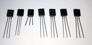
Waiting for ordered 75K for R9, 10 I'm considering replacing JFET in my two SSHV2. I've measured JFET' IDSS my spare 2SK117s and the strongest I have got are: 4.9 and 4.1mA.
Do you think I could have better Vout regulation around 350V if I replaced JFETs also? Currently I have soldered JFETs with IDSS 3.4 ~3.5mA
Yes, it is the best option.Thanks Laurent33.
...I'm considering replacing JFET in my two SSHV2. I've measured JFET' IDSS my spare 2SK117s and the strongest I have got are: 4.9 and 4.1mA.
Do you think I could have better Vout regulation around 350V if I replaced JFETs also? Currently I have soldered JFETs with IDSS 3.4 ~3.5mA
Waiting for ordered 75K for R9, 10 I'm considering replacing JFET in my two SSHV2. I've measured JFET' IDSS my spare 2SK117s and the strongest I have got are: 4.9 and 4.1mA.
Do you think I could have better Vout regulation around 350V if I replaced JFETs also?
Yes, that will go the right direction to.
For the same reasons, I ordered some 2SK117 BL. I'll try that soon.
Laurent
Hi it is good idea to change standard solen 10uf anf 0.33uf capacitor to better for exemple mundorf evo alu foil ? Thanks
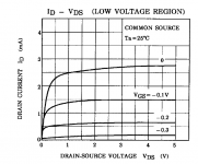
Saturation area or not ?
Hi Salas,
Been playing around with 2SK117BL, IDSS 8+mA. Result was terrible, ref voltage was too high at startup spoiling completely the CCS spare voltage then settling down after a minute at the right voltage 25v lower.
So, took some time to understand better FET behavior regarding Temperature Coefficient to find out that BL FET was way too much in the negative coef area at such low current / low VDS.
I measured several GR and BL to find where was the "zero" coef point at different VDS/ID combinations. So plenty measurements, as much possibilities to chose from but I wonder one thing (at a time), I have an idea but would like confirmation :
I did not measure Q5 VBE, last time I tried I popped several silicons, but from simulation it's around 0.5V. Having Q6 VGS at 0.18V, that leave just 0.32v for Q6 VDS. The FET is obviously not biased in it's saturation area. "from the books" that would give poor regulation to the CCS made by Q6 regarding PS noise rejection. Does that way to bias it is a second order matter having it fed by the regulated voltage and backed up by C2 ? Don't know if I make myself clear enough.
Having it biased after the knee, VDS at 2v minimum, and at the same time close to the zero T° coef would need more than double current, obligatorily switch to BL to keep some VGS to deal with, close to 1.5w to dissipate in each R9, R10 and a necessity to drop some diodes (leds or regular ones) on top of Q5 to get the right voltage drop. So I wonder if there's a point to go that way, not even thinking about thermal behavior of the diodes.
Right now with a small current increase (2.9mA) I could be at the zero point with some high IDSS GR I got, that should be more stable Vs T° variations. Probably less hassle.
By the way, I think I will try to install the FET below the board, far from Q5. 🙂
Laurent
I ordered some 2SK117 BL. I'll try that soon.
Hi Salas,
Been playing around with 2SK117BL, IDSS 8+mA. Result was terrible, ref voltage was too high at startup spoiling completely the CCS spare voltage then settling down after a minute at the right voltage 25v lower.
So, took some time to understand better FET behavior regarding Temperature Coefficient to find out that BL FET was way too much in the negative coef area at such low current / low VDS.
I measured several GR and BL to find where was the "zero" coef point at different VDS/ID combinations. So plenty measurements, as much possibilities to chose from but I wonder one thing (at a time), I have an idea but would like confirmation :
I did not measure Q5 VBE, last time I tried I popped several silicons, but from simulation it's around 0.5V. Having Q6 VGS at 0.18V, that leave just 0.32v for Q6 VDS. The FET is obviously not biased in it's saturation area. "from the books" that would give poor regulation to the CCS made by Q6 regarding PS noise rejection. Does that way to bias it is a second order matter having it fed by the regulated voltage and backed up by C2 ? Don't know if I make myself clear enough.
Having it biased after the knee, VDS at 2v minimum, and at the same time close to the zero T° coef would need more than double current, obligatorily switch to BL to keep some VGS to deal with, close to 1.5w to dissipate in each R9, R10 and a necessity to drop some diodes (leds or regular ones) on top of Q5 to get the right voltage drop. So I wonder if there's a point to go that way, not even thinking about thermal behavior of the diodes.
Right now with a small current increase (2.9mA) I could be at the zero point with some high IDSS GR I got, that should be more stable Vs T° variations. Probably less hassle.
By the way, I think I will try to install the FET below the board, far from Q5. 🙂
Laurent
Hi Laurent,
That is why I specified GR vs BL. I had tested those matters during the development back then. Don't expect such low noise Jfets to have great tempco even when best chosen though. A J201 was more stable but noisier for instance. Low current type with higher output conductance is always steadier but noisier. Showing up clearly in the noise floor of some very quiet MC phono bumping it up but maybe acceptable in your application.
Under one Vbe the GRs just offer better impedance (but not great impedance) than using say a 250-300 Ohm resistor for 2mA. But the resistor (or trimmer) will be single active parameter affected in its current delivery since I=Vbe/R. Which may prove less susceptible to the board & box thermal environment.
I had shown some K117 traced curves and done some delta measurements with stepping down VDS at a point much time ago but it should have been in the low voltage threads. To keep a long story short the GRs appear just above the knee clearing the resistive region but not in full saturation region. In between. For Vbe as VDS that is. Everything is a compromise as you have pointed out like when I had lifted the VDS with diodes and the output impedance suffered in the lows or it would have been high dissipation in the Ref resistors because without more Id its half baked. If you put Zeners instead they need even more mA and they are very noisy and have a spectrum color in that too. Then you go electrolytic, you get the picture. This one reg was a balancing act to get a nice sound different than from the usual stuff with few components and only passable thermals because in HV settling for few volts its very small %. But noise and Zo better than passable. I recommended you try the resistor only thing again earlier in our discussion If memory serves right.
Thanks Salas, I see you have been thru the long process of optimization of a robust design.
All I need is to get rid of the thermal as much as possible or at least master it enough to make it symmetric between the two positive and negative supply.
I will keep it simple. I will continue to play with the GR as I want to make use of the measurements and give a try to the resistor trick in between.
You've got accurate memory Salas, so that question is a bit touchy: Are you sure for J201, it has IDSS between 0.5 and 1.0mA, maybe J202 ? 😀
Laurent
Laurent those figures you saw in the datasheet but maybe I still got some J201 samples somewhere let me dig them up and I will measure them for you. Vref resistors value easy to change when its good to use the lowest Vgs (off) J type.
He, he, I dug few up. J201 is a stable guy indeed but below 1.5V it loses uA fast when pressed between fingers while even a 4mA K117GR can be steady at 0.6V VDS in that rough test. Because J201 can have around -0.9V pinch off even at 0.75mA idss when the 4mA GR had -0.5V only. J201 Fairchild and NOS National random samples were well consistent for idss. 2SK117GR lowest possible idss samples and used as near to 0 Vgs remains the best choice in this situation. 😉
Attachments
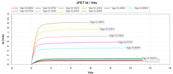
Nice curves, very linear in positive VGS.
I'll remember my last resort is in the resistor.🙂
Thanks Salas, clever advice.
Laurent
As a general figure, pinch off occurs at a smaller VDS with K117, so right, better stick with K117.Because J201 can have around -0.9V pinch off even at 0.75mA idss when the 4mA GR had -0.5V only.
OK, having VGS near 0 leaves the voltage drop almost totally for VDS, allowing to be as close as possible to the saturation area. I have one GR sample at 2.7mA IDSS, I'll give it a try at 1.8mA which is my current setting. I also ordered Y version to see if it's getting better with even a closer IDSS to my target. All that looking for the zero tempco of course.2SK117GR lowest possible idss samples and used as near to 0 Vgs remains the best choice in this situation. 😉
I'll remember my last resort is in the resistor.🙂
Thanks Salas, clever advice.
Laurent
Vgs is really a negative number in NJFET polarity. Its this tracer working with positive Vgs number figures in Id/Vgs. Although it knows to put a minus in the test page and in the Id/Vgs tracing page. We can mentally adjust maybe but they could fix it in the software. If asking it to start from a minus it only traces zero. So it must be the hardware doing one way bias. I will contact them to know if they can use another display way.
Y grade is a good test idea when you can can find originals of them.
Y grade is a good test idea when you can can find originals of them.
Attachments
Y grade is a good test idea when you can can find originals of them.
Found them on the bay, at least the box which contain the 2000 FETs looks original. Marking is a bit different from what I have. From PRC, will see.
Hi all,
I have built 2 pieces of SSHV2 supplying a (relatively) lowish voltage (175V output) for a balanced Aikido noval. Worked like a charm from the start, both, so praises should go to Salas, the builders and contributors. I only use a tube rectifier with 10H choke and 2x15uF MKP caps at the input.
During the setup of the stage I connected a discharged 10uF cap across the live load and that killed the SSHV... well, a bit of a surprise, as according to my knowledge a shunt regulator is inherently protected at short circuits. I took me like 20 minutes to debug the issues in the circuit, and Q5 and Q6 were fried (shorted). Much more time to replace them, as the PCB is double sided...
Later, during fine tuning of the supply voltage, i did it again 🙁 I shorted the supply lines with one of the DMM probes. Same culprits, the JFET and the top bipolar from the shunt, and additionally the protection Zener (D3) was as well destroyed. All fixed now, but the PCB was a bit damaged (collector pad of Q5 from the top does not exist anymore which required a separate strap to connect it with emitter of Q4)
I wonder if anybody else have had similar experiences when shorting the output? Also, what could likely be the cause of damaging (systematically) of the Q5 and Q6 when output goes to 0? It seems that E-B junction of Q5 goes shorted (few ohms measured both directions) but as well it shorts the gate junction of 2SK117.
I assume it's the C2 (charged at almost the output voltage) that reverse biases Q5(B-E) and Q6 when Output goes to 0, while D3 is too slow to protect.
In this case maybe an ultra fast diode in parallel with the Zener do you think it would help? I think the Zener is protected by the B-E junction of Q5 ( 😀 ), but I guess the role of Zener is to prevent something more catastrophic.
I know, I have to be more careful (and I will be) but I am very curious to hear some feedback from Salas or others that have been through similar experiences.
Cheers!
Its not that the CCS does not limit the incoming current, its the C2 charge that does the little semis killing job when you short as you described. The Zener was put there for start up time protection of Q6 supposedly, but it surely can't protect the small semis in output shorts. That is why there is no instruction in the guide that you may short the output without some damage. With a 1N4148 in its place there is no change for normal operation so you may try it.
Its not that the CCS does not limit the incoming current, its the C2 charge that does the little semis killing job when you short as you described. The Zener was put there for start up time protection of Q6 supposedly, but it surely can't protect the small semis in output shorts. That is why there is no instruction in the guide that you may short the output without some damage. With a 1N4148 in its place there is no change for normal operation so you may try it.
Thanks Salas! I guess, though, that 1N4148 is somewhat tiny for that job. This device should offer a safe path to discharge C2 in case of a short. I will try to bypass the Zener with a bigger Schottky and report back!
Sent from my iPhone using Tapatalk
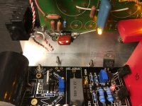
Ok, problem solved [emoji16] . I have soldered half of SBL1640 on top of the Zener (this is what I had on hand) and the regulator survived successfully several short circuits.
I have added 2 pictures to show more exactly what I have done.
I have added 2 pictures to show more exactly what I have done.
Attachments
Last edited:
- Home
- Amplifiers
- Power Supplies
- Simplistic mosFET HV Shunt Regs