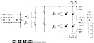
Hi, is there an argument against the following snubber configuration (C1, C2, R1)?

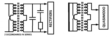
What would be the right connection of the transformer to the Quasimodo jig in order to optimize the component values for it?
What would be the right connection of the transformer to the Quasimodo jig in order to optimize the component values for it?
Attachments
Last edited:
You should look it up in the manual, page 11, fig. 13: „all“ Quasimodo configurations.
The snubber looks good to me, but only Q will tell you the precise correct values. (Or look if it’s already been done for your transformer, „Quasimodo results only“
The snubber looks good to me, but only Q will tell you the precise correct values. (Or look if it’s already been done for your transformer, „Quasimodo results only“
Sinigersky, for that particular circuit configuration you are not snubbing across just the section of winding that is being commutated. In your schematic the snubbing current forced by one section of winding being commutated has to also pass through the other secondary winding before it gets back to the winding that is being commutated.
You should look it up in the manual, page 11, fig. 13: „all“ Quasimodo configurations.
Well, I am asking this question just because I did not find the answer in the manual. 🙂
Sinigersky, for that particular circuit configuration you are not snubbing across just the section of winding that is being commutated. In your schematic the snubbing current forced by one section of winding being commutated has to also pass through the other secondary winding before it gets back to the winding that is being commutated.
I might be wrong, but I thought in this configuration two diodes "commutate" simultaneously, in pairs, both secondary windings. I.e. D1 + D4 switch off both in one moment, then in a later moment, D2 + D3 switch off, and so on. The two ends of the secondary windings, which are not connected together, should be ringing in a "balanced" manner with opposite polarities, and the snubber (as shown) should be effective for this ringing, too. Or do you see an error in this explanation?
I would have assumed that this configuration is the right one to use with the jig:

The issue is that there is a separate entry in Fig. 13 for the "center tapped secondary" which suggest that two snubber groups should be used. I was trying to understand what is a possible problem with the single-snubber configuration from my post above.
The issue is that there is a separate entry in Fig. 13 for the "center tapped secondary" which suggest that two snubber groups should be used. I was trying to understand what is a possible problem with the single-snubber configuration from my post above.
Attachments
Although it may appear that both sides are balanced, there are always real world differences to winding resistances and leakage inductances, and filter capacitance values, and load currents for each polarity. Those differences can lead to different commutation instants.I might be wrong, but I thought in this configuration two diodes "commutate" simultaneously, in pairs, both secondary windings. I.e. D1 + D4 switch off both in one moment, then in a later moment, D2 + D3 switch off, and so on. The two ends of the secondary windings, which are not connected together, should be ringing in a "balanced" manner with opposite polarities, and the snubber (as shown) should be effective for this ringing, too. Or do you see an error in this explanation?
But even so, the issue is to follow the transient current flow loop that a particular winding generates as its related diodes turn off - that loop should be bypassed by its own snubber, rather than have to take a long path around and through the other winding.
BTW, as I understand the Introduction, we're supposed to get to ζ > 1 (overdamp the beast and thus go further than critically damp it), I still can't quite relate the "optimal" curve as the "target" and not just the "starting point"? Or not? Do we aim ζ ≥ 1 ?
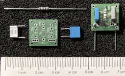
Adjust the pot to find the R value that gives the shape in the photo above. It’s that simple.
Also, a little less R, meaning slightly less damping, is better than too much.
What about 2 snubber sets since there are 2 secondary windings ? 🙂
What about saving some space on the PCB, and some cost? 🙂
But if it is evident that this is a really bad idea, I will have to re-design / re-consider things.
Attachments
You need to convince yourself first - perhaps do some testing - or try to understand the basic operation of the snubber and what the leakage inductance current loop is doing and why.
Your transformer and rectifiers use a center tapped arrangement. Thus you need two C+RC snubbers as shown in the bottom row of Figure 13 on page 11 of the Quasimodo design note.
Adjust the pot to find the R value that gives the shape in the photo above. It’s that simple.
Also, a little less R, meaning slightly less damping, is better than too much.
Thank you, 6L6
Step up Transformer
Good day everybody,
I want to regnerate AC mains with an amp and a step up transformer on its output.
Besides inrush current I am a little worried about switch off voltage spikes from the transformer on each side.
Can I use the Quasimodo to design a primary and secondary snubber for the step up transformer? Should I add varistors across the primary/secondary as well?
Many thanks
Ozo

That will lower the resonant frequency, but not provide the necessary damping. It's the 'R' in the 'C+RC' that consumes the oscillatory energy.
There will definitely be switch-off spikes on the step-up secondary. But Quasimodo doesn't clamp the spikes (which might be a good thing, worth doing 😉). It only absorbs the energy stored in a transformer's leakage inductance when the rectifiers on its secondary commutate, reducing generated EMI. Your design challenge is a bit different, since your step-up secondary won't get rectified until it passes through another transformer (presumably).
The 0,22 uF capacitor across the secondary will be a substantial additional load on the amp output, even if the step-up ratio is only 2: or 3:1.
Cheers
Last edited:
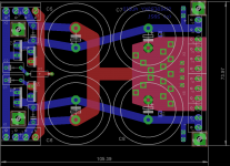
Beautiful! Any plans to make a batch and sell 'em? 😀 (thinking of just the boards)
I'd be surprised if there aren't other fellers out here that'd be interested -- besides me, of course!
But then, it can be a very time-consuming undertaking.
Cheers
I'd be surprised if there aren't other fellers out here that'd be interested -- besides me, of course!
But then, it can be a very time-consuming undertaking.
Cheers
Last edited:
Hi Rick,
thanks for the cudos!
A WW group buy would be beyond my time allocation possibilities. If there's sufficient interest, I could ask @Prasi if he's interested to offer it, maybe he'd be interested, as he offers ideal bridge rectifier boards as well.
Greetings,
Winfried
thanks for the cudos!
A WW group buy would be beyond my time allocation possibilities. If there's sufficient interest, I could ask @Prasi if he's interested to offer it, maybe he'd be interested, as he offers ideal bridge rectifier boards as well.
Greetings,
Winfried
- Home
- Amplifiers
- Power Supplies
- Simple, no-math transformer snubber using Quasimodo test-jig