Somebody asked "please write out the mathematics which calculates the power dissipated in the snubbing resistor" in early October of 2018. I think if you go review postings in this thread from that period of time, you'll definitely find one with ALL the math. Then you can calculate the AC power dissipated in the snubbing resistor. Member 6L6 has already pointed out that the DC power dissipated in the snubbing resistor, equals zero microwatts. Thanks to the absence of a DC current path.
The AC power dissipated in the snubbing resistor(s) can become surprisingly non-negligible, especially in vacuum tube circuitry where the transformer secondaries are > 150VAC.
Of course the modern, year 2021, approach to calculation is to enter the circuit topology into a circuit simulation program like SPICE, then let it do all the work. You can do that. Every diyAudio member can do that.
_
Last edited:
The resistor is attached to a capacitor in series.
Ah, I just calculated the reactance of the 0.01uF cap for 60Hz input, and it is 265K ohms. So that should be fine then!
The resistor is attached to a capacitor in series.
Ah, I just calculated the reactance of the 0.01uF cap for 60Hz input, and it is 265K ohms. So that should be fine then!
Cap value should be 0.15uF, so reactance is 17.68K ohms, still negligible current draw in my case (~1mA).
Hi,
thanks a lot for making it possible to determine the snubber values with the QUASIMODO tool, especially to Mark Johnson.
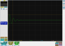
First measure with my new RIGOL 1054Z, without variable resistor Rs:

Ronny
thanks a lot for making it possible to determine the snubber values with the QUASIMODO tool, especially to Mark Johnson.
First measure with my new RIGOL 1054Z, without variable resistor Rs:
Ronny
Great job Ronny! Since you've got the two channel display, you definitely want to set the scope to trigger upon the yellow-trace channel's falling edge. Being a perfect square wave, it is completely unambiguous where the trigger event MUST be. Unlike the blue waveform, the yellow doesn't ring-a-ding-ding above and below the potential trigger level.
_
_
Last edited:
Cap value should be 0.15uF, so reactance is 17.68K ohms, still negligible current draw in my case (~1mA).
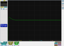
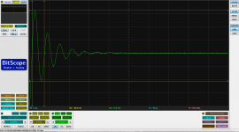
I found out that I forgot to short out the primary side of the transformer before the measurement. Once it is shorted out, the snubber resistor value is now at 47 ohms instead of 10 ohms. I also used ch 1 to trigger on the falling edge of the pulse and ch 2 to do the measurement. Here are the screen shots:
Vertical division is 5v before the adjustment. Vertical division is 1v after the adjustment.
Many thanks to Mark Johnson for making this circuit available to us DIYers 🙂
Attachments
I will soon order some V4 thru hole boards, and parts in the weeks to come.
I am living in The Netherlands in case anybody would like to lean on my order.
After some days I'll decide how many will be ordered.
Related to that, the MOSFET in the original design (NTD4906N, IPAK package) and the listed substitutes in later BOM (IRLB8748 and IRLU8726, both TO-220 package) are no longer available at Mouser.
So I did a survey based on the required parameters provided by Mark in an early post, and found some suitable available substitutes:
- IPAK package: AUIRFU8401 (end of life, by the way)
- TO-220 package: IRLB8721 and IPP055N03L
Attachments

Last edited:
I looked through the results thread and couldn't find any results for an Antek AS-4220. Does anyone have any results for it?
Very nice work @Osuka, congratulations! I'm sure any of those will work extremely well.
Trying to recall from the dark recesses of ancient memory: back in summer 2013, I used DigiKey parametric search to choose devices. First I limited the search to N-channel transistors in thru-hole packages, then I further limited it to those rated 30V or higher for VDS, then (RDSon <= 50 milliohms), then (QGtotal <= 40 nanoCoulombs)
This whittled down the universe of possibilities to a few hundred. I clicked the button on DigiKey's site which downloads the whittled-down table in spreadsheet (.csv) format. Then I opened the spreadsheet and created a new column: Mark's Figure Of Merit, which was (QGtotal * RDSon). I wanted low gate capacitance for easier drive, and most rows in the spreadsheet had a number for QGtotal. (Far more than had a number for capacitance itself). I also wanted a low on-resistance. So (QG * OnResistance) is a quantity that measures "how bad is this device". Equivalently, [1 / (QG * OnResistance)] measures "how good is this device". Sort by the figure of merit and pick devices whose Figure Of Merit is the most desirable. At that time, eight years ago, the ON Semiconductor NTD4906 was the winner. Today I'm sure there would be a new champion.
This is of course a totally unnecessary micro-optimization since the gate of the MOSFET is driven by a special purpose MCP1407 chip rated for SIX AMPERES. But what's the harm of buying the best possible MOSFET and ALSO driving the excrement out of it? Easy and fun.
It seems we here just see a glimpse of Mark’s methodical genius.
I mean, this is awesome as a method.
I mean, this is awesome as a method.
Trying to recall from the dark recesses of ancient memory: back in summer 2013, I used DigiKey parametric search to choose devices. First I limited the search to N-channel transistors in thru-hole packages, then I further limited it to those rated 30V or higher for VDS, then (RDSon <= 50 milliohms), then (QGtotal <= 40 nanoCoulombs)
Thanks Mark. I went trough a similar selection process, and was then thinking: what would make one device better than the other for this little test gear? For sure that the low test frequency and high current availability wouldn't impact the slew rate of the test signal, but some devices may have tens of nanoFarads capacitance, which may end up as an undetected 'result bias', I was thinking, while we would like our test gear to have ideal properties that do not influence the measurement.
So I went for the C(OSS) capacitance as it is in parallel with the transformer under test. But yes, taking the total energy storage/discharge in the entire MOSFET is perhaps the best way to define the inherent device quality.
Oscar
Last edited:
I don't think DigiKey put C(OSS) in their parametric selection tables back in 2013.
In any case the prototype worked beautifully with only 100mA of gate drive (from five 74AC14s in parallel), and with the world's crappiest FET: three 2N7000s wired in parallel, and with only a 5V power supply to charge the MOSFET gate. Despite all that, the prototype worked very well.
So the subsequent V4 revision, which increased the supply to 9V, and 6000mA of gate drive, and a very good FET, was an improvement. But not a gigantic one.
Which pages of the Design Note did you read, and which pages did you not read?
Read pages 1-15
Metalized film caps mentioned on page 7 it is, will go with those.
Got the snubber R value for Triad VPS10-2500 transformer, though I'd share it with the forum members:
R=96.2 ohms, so 100 ohms is used.
Cx=0.01uF
C2=0.15uF
R=96.2 ohms, so 100 ohms is used.
Cx=0.01uF
C2=0.15uF
Snubber resistor for FirstWatt SIT-3 amp?
I opened up my FirstWatt SIT-3 amp and did some unsoldering and soldering so I can get to the secondary side of the transformer. There is no snubber in the circuit at all. Bridge rectifier used is the the GBPC3502, which is available from a number of manufacturers.
I shorted the 2nd set of transformer secondary winding while measuring the 1st set. It has two identical secondary windings for the left and the right channel.
I had to solder some bridging wires to make sure the primary side of the transformer is indeed shorted. There is a circuitry from the AC receptacle to the transformer's primary, so I'm not sure if shorting the pins on the AC receptacle and turning on the power switch is enough.
I got:
R=10 ohms
Cx=0.01uF
C2=0.15uF
The ring freq is around 806KHz when R=1K ohms.
I'm a bit leery that R is this low. Prior to this, I measured 3 transformers, and they have anything between 47 - 120 ohms.
Has anyone come across any transformer with such low R value for the snubber?
Attachments
Search for the thread whose title is Quasimodo results (ONLY)
There are tons and tons of (Transformer_Model_number, Cx, Cs, Rs) datapoints listed
No chitchat, no requests, no off-topic posts: just results (ONLY)
There are tons and tons of (Transformer_Model_number, Cx, Cs, Rs) datapoints listed
No chitchat, no requests, no off-topic posts: just results (ONLY)
I'm building a single-ended EL84 amp based off a PCB of my own design (first attempt at a PCB), and have been chasing a high frequency ringing that is only present on one of the channels.
After trying many things, the two that have been most effective in cleaning up that ringing is either snubbing the high voltage secondary, or using regulated DC instead of AC for the heaters.
The ringing issue aside, the amp is quieter with the regulated DC heaters, than AC heaters with snubbers across the HT secondary, so that is a change that I will make permanent.
That said, I am fairly certain the transformer was making less mechanical noise with the snubber in place, so I'd like to do that as well.
For temporarily snubbing, I used a 0.1uF cap in series with a 1.2K resistor across the two secondary wires. (I measured 1.2K with Quasimodo Jig, although that was with different Cx and Cs values).
My experiment was far from optimal but still had some positive effect, both in reducing the HF ringing and mechanical transformer noise.
The improvement in ringing was observed both on an oscilloscope and PC-based spectrum analyzer.
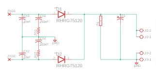
Based on figure 13 in the Quasimodo paper, for a center tapped transformer (mine is Hammond 270HX, 550 VCT), there should be dual C-RC snubbers, from each secondary to the CT.
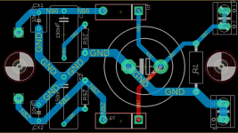
I have a draft for a PCB to hold the snubbers, rectifier diodes and 220uF main filter cap.
It would be great if someone can double-check that the layout is correct, along with any other improvements or suggestions to the layout.
The mounting holes and PCB size are intentional, to fit on top of the power transformer mounting tabs.
edit: also wanted to mention the rectifier diodes I chose are TO-247 soft-recovery ISL9R30120G2 (Mark's "belt and suspenders" approach).
I assume that at 30A rating, they won't need heatsinking for the 100mA B+.
After trying many things, the two that have been most effective in cleaning up that ringing is either snubbing the high voltage secondary, or using regulated DC instead of AC for the heaters.
The ringing issue aside, the amp is quieter with the regulated DC heaters, than AC heaters with snubbers across the HT secondary, so that is a change that I will make permanent.
That said, I am fairly certain the transformer was making less mechanical noise with the snubber in place, so I'd like to do that as well.
For temporarily snubbing, I used a 0.1uF cap in series with a 1.2K resistor across the two secondary wires. (I measured 1.2K with Quasimodo Jig, although that was with different Cx and Cs values).
My experiment was far from optimal but still had some positive effect, both in reducing the HF ringing and mechanical transformer noise.
The improvement in ringing was observed both on an oscilloscope and PC-based spectrum analyzer.
Based on figure 13 in the Quasimodo paper, for a center tapped transformer (mine is Hammond 270HX, 550 VCT), there should be dual C-RC snubbers, from each secondary to the CT.
I have a draft for a PCB to hold the snubbers, rectifier diodes and 220uF main filter cap.
It would be great if someone can double-check that the layout is correct, along with any other improvements or suggestions to the layout.
The mounting holes and PCB size are intentional, to fit on top of the power transformer mounting tabs.
edit: also wanted to mention the rectifier diodes I chose are TO-247 soft-recovery ISL9R30120G2 (Mark's "belt and suspenders" approach).
I assume that at 30A rating, they won't need heatsinking for the 100mA B+.
Attachments
Last edited:
Umm, sadly, though, a 30A rectifier will dissipate only slightly less power than a 1 or 2A rectifier if providing the same current. The temperature rise will be slightly less due to the greater thermal mass and dissipating surface area.
100mA rectified, shouldn't be too hard to shake off the BTUs, though.
Cheers
100mA rectified, shouldn't be too hard to shake off the BTUs, though.
Cheers
Last edited:
- Home
- Amplifiers
- Power Supplies
- Simple, no-math transformer snubber using Quasimodo test-jig