How to know if mute is needed or not?To input pcm2dsd you must connect: data, bclk, lrck, mclk and dsdon.
And if you need mute.
🙂 You must know, your "dac" needed?How to know if mute is needed or not?
Yes I know you are right, 1st let me try PJotr25 combination Amanero-Cronus-pcm2dsd-lpf, later will clean and surely I will change to a bigger box, thanks Mark.IIRC Chronus DCK is BCLK (data-clock / bit-clock). Easy to check clock frequency with a scope to make sure. D1 and D1 would be either LRCK and DATA for PCM, or else DSD_L and DSD_R for DSD mode. Check with scope if not sure which one (D1 or D2) is LRCK.
EDIT: I would still recommend to clean up layout and wiring. Its way too disorganized for RF. Transformers/inductors are too close to RF, etc. Think of a clean layout in terms of signal flow, keep I2S wires as SHORT AS POSSIBLE. Move boards around to make I2S and MCLK wire lengths very short and direct. Also, twisted pair wires have high characteristic impedance than 50-ohms. Probably closer to 100-ohms. You may need to add some damping resistors (maybe try 50R metal film) in the I2S lines where the impedance in changing to achieve best waveform fidelity. Ground scope probes carefully with short ground leads and use a fast enough scope. Otherwise the scope and probes will distort the waveforms you see so what you see will not be accurate.
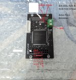
On pcm2dsd input is marked as "Amanero", output is marked as "DSC".
So from cronus connect to "Amanero".
So from cronus connect to "Amanero".
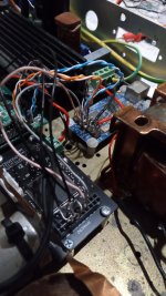
I don't see much in this mess... But possibly a gray wire connect mclk from Amanero to DSDOn pcm2dsd, but I'm not sure... Maybe better photos...It's connected, attached pic.
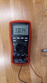
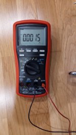
But if it is well connected check if DSDON is "0" if play pcm and "1" if play dsd.
Your connections look bad.0 VAC is PCM & 1 VAC is DSD?
They may not work correct.
You have to change it to be sure of connections...
Maybe let's go to priva because it does not apply to the thread...
It should be VDC, not VAC. DC voltage levels are usually close to ground (0vdc) for a low, and close to Vcc/Vdd for a high (around +3vdc). A low is most often taken to mean a logic 0 and and high is most often a logic 1. In this case logic 0 can also represent 'false,' and logic 1 can represent 'true.' However there is also inverted logic where a 0v = true = logical 1, and similarly inverted for logic 0. Anyway, the point is that logic 0 and logic 1 are Boolean algebra logic numbers and not the same thing as voltages.
Last edited:
I've had PCBs for this since you guys originally posted your design - then parts availability became a problem and I haven't touched it. Many places now show the Xilinx processor as discontinued but a quick search showed this place as apparently having stock - is it the correct part? Not sure if it can be assumed the parts will be genuine - anyone able to comment?
https://www.lcsc.com/product-detail...LDs-FPGAs_XILINX-XC6SLX9-2TQG144C_C27408.html
https://www.lcsc.com/product-detail...LDs-FPGAs_XILINX-XC6SLX9-2TQG144C_C27408.html
- Home
- Source & Line
- Digital Line Level
- Simple DSD modulator for DSC2