The mixed clock domains and long wires might be part of the noise problem. Maybe noise on the I2S bus is causing false triggering in the FPGA inputs or something. You could try looking at I2S signals into and out of simple DSD converter with the scope to see if they look like they should. Also check power supply voltages and noise. Other than that it only makes sense to clean up the layout and clocking. Its bad enough right now that it could be causing various problems, or possibly making other problems even worse.
EDIT: Agree with PJotr25 to try removing Chronus. It may be doing more harm than good under the circumstances.
EDIT: Agree with PJotr25 to try removing Chronus. It may be doing more harm than good under the circumstances.
Yes, it's connected Amanero (clock slaved from Cronus 22/24Mhz) to pcm2dsd to Cronus to LPF.As i can see there are two domains, one amanero + pcm2dsd and second Cronus + dac.
For me better connect: Amanero in slave mode (mclk from cronus if cronus have clock 22/24MHz) -> cronus -> pcm2dsd -> dac.
Remember that pcm2dsd requires mclk from the 22/24MHz family.
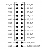
Cronus DSDON output is DCK output?
It's a lot of work: Amanero is Cronus slavedDisconnect cronus, and connect pcm2dsd directly to dac and see if the noise has changed.
I guess is better to connect directly with the 20 pin connector the Amanero to the Simple DSD Modulator & by software come back to unslave the Amanero (Slave_1081_DSDSWAPPED e firmware_2006be11 PIN6 MCLK input per selezionare il CLOCK devi cambiare il PID_071A in PID_0a23 e abilitare il selettore PIN 1 o PIN 11) someone remember with soft to flash for unslaved Amanero?
Remove Cronus or connect Amanero in slave mode with Cronus and after them pcm2dsd.
Pcm2dsd no slave mode on output. Mclk connect to pcm2dsd only in input.
Pin DSDOn on Amanero it is "1" if play DSD, "0" if play PCM.
Pin DSDOn on Pcm2dsd always it is "1". It is signal for run dac DSC.
Pcm2dsd no slave mode on output. Mclk connect to pcm2dsd only in input.
Pin DSDOn on Amanero it is "1" if play DSD, "0" if play PCM.
Pin DSDOn on Pcm2dsd always it is "1". It is signal for run dac DSC.
OK I do Amanero in slave mode => Cronus => pcm2dsd.
Not clear how to connect Cronus to pcm2dsd?
Pcm2dsd output analog left channel pin 9 LRCKOUT & analog right channel pin 5 DATAOUT + of course pin 6 & 10 both GND?
Not clear how to connect Cronus to pcm2dsd?
Pcm2dsd output analog left channel pin 9 LRCKOUT & analog right channel pin 5 DATAOUT + of course pin 6 & 10 both GND?
Attachments

Last edited:
OK I do Amanero in slave mode => Cronus => pcm2dsd.
Not clear how to connect Cronus to pcm2dsd?
Pcm2dsd output analog left channel pin 9 LRCKOUT & analog right channel pin 5 DATAOUT + of course pin 6 & 10 both GND?
Attachments
Cronus outputs feeding my LPF are D1 right channel & D2 left channel. MCK output goes to Amanero.
I don't understand you: after the pcm2dsd I only need the analog left & right channel to be filtered with my low pass filter or in your case your DSC???
From pcm2dsd you have DSD signal. DSD signal it is left & right (lrck & data) and dsd clock (bclk).
And eg. for DSC additionally connect mute & dsdon.
And eg. for DSC additionally connect mute & dsdon.
Ok make sense, so as I saidFrom pcm2dsd you have DSD signal. DSD signal it is left & right (lrck & data) and dsd clock (bclk).
And eg. for DSC additionally connect mute & dsdon.
IIRC Chronus DCK is BCLK (data-clock / bit-clock). Easy to check clock frequency with a scope to make sure. D1 and D1 would be either LRCK and DATA for PCM, or else DSD_L and DSD_R for DSD mode. Check with scope if not sure which one (D1 or D2) is LRCK.
EDIT: I would still recommend to clean up layout and wiring. Its way too disorganized for RF. Transformers/inductors are too close to RF, etc. Think of a clean layout in terms of signal flow, keep I2S wires as SHORT AS POSSIBLE. Move boards around to make I2S and MCLK wire lengths very short and direct. Also, twisted pair wires have high characteristic impedance than 50-ohms. Probably closer to 100-ohms. You may need to add some damping resistors (maybe try 50R metal film) in the I2S lines where the impedance in changing to achieve best waveform fidelity. Ground scope probes carefully with short ground leads and use a fast enough scope. Otherwise the scope and probes will distort the waveforms you see so what you see will not be accurate.
EDIT: I would still recommend to clean up layout and wiring. Its way too disorganized for RF. Transformers/inductors are too close to RF, etc. Think of a clean layout in terms of signal flow, keep I2S wires as SHORT AS POSSIBLE. Move boards around to make I2S and MCLK wire lengths very short and direct. Also, twisted pair wires have high characteristic impedance than 50-ohms. Probably closer to 100-ohms. You may need to add some damping resistors (maybe try 50R metal film) in the I2S lines where the impedance in changing to achieve best waveform fidelity. Ground scope probes carefully with short ground leads and use a fast enough scope. Otherwise the scope and probes will distort the waveforms you see so what you see will not be accurate.
Last edited:
Yes, Markw4 is absolutely right, it is very important...I would still recommend to clean up layout and wiring. Its way too disorganized for RF. Transformers/inductors are too close to RF, etc. Think of a clean layout in terms of signal flow, keep I2S wires as SHORT AS POSSIBLE. Move boards around to make I2S and MCLK wire lengths very short and direct.
- Home
- Source & Line
- Digital Line Level
- Simple DSD modulator for DSC2