Did the schematic of the Elektor buffer
Wanted to proceed from schematic to PCB, and thence to Enlightenment.
Is this schematic okay? One newbie question: with discrete circuits like this with less-than-opamp level PSRR, does crosstalk increase because of supply rails-based coupling of channels? And therefore is there any concept of "decoupling" each channel of the buffer, like we do with opamps (though there it's to stop oscillations, I think).
I've put two pairs of caps at the point where the supply lines enter the PCB.
Once you comment on the schematic, I'll pass it to the PCB stage. I've already done the PCB layout based on the current schematic.
Tarun
Attachments

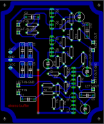
And here's the PCB... couldn't wait
The PCB is supposed to be single-sided. The single top-surface track will actually be implemented as a jumper wire. Other than that, there's nothing very revolutionary. Sorry if my total lack of PCB layout skills is showing up. It was done using the free version of Eagle, with manual place and route.
Tarun
Attachments
I had some of the original boards ( leftovers ) but I can't find them anymore. I guess they ended up in the bin, you can't stock everything. Built some of them at that time and I was satisfied with the quality IIRC. We used 4.7 uF for output caps and a 100 Ohm series resistor to the RCA's. Power supply was an Elektor board with the good old Exar XR4195CP +/- 15 V DIL8 dual regulator which was not bad at all ( I did find 10 of those ). The original PCB's did not have decoupling at all and I recall soldering decoupling caps on the boards. Discussion on cap-quality for the 10 uF 16 V was hot those days....
Nowadays a Wima 10 uF 16 V MKT with 5 mm pitch will fit !
Can you attach the Eagle files please ? The board looks OK and for once I see someone making room for standoffs for mounting the board. A big hurray for that. I would cut the ground track however so that only one track will be the ground instead of a ring-ground. Swapping C10 and R13 might be a good idea, C12 can be mounted horizontally that way.
Resistors used for the cascoding transistor biasing have generally too low values. Use the higher values thus the cap can be smaller, say 1uF. Shown biasing scheme will, btw, provide not much more than the minimal necessary swing (usage of the JFET without biasing resistors, be it high Vgs or not, will btw have the same problem), try to tune cascoding transistor’s voltage (base and emitter) somewhere in the middle of the Vcc. With BJT as cascoding device, one might use exclusively its base current and relatively high value resistor and reference it to the positive supply only.
At the other hand, base stopper is probably too high and as such reduces the effect of the cascoding. However, some base stopper still should be used, and especially should be used to prevent peaking/oscillations caused by the non-zero signal source impedances.
If this can be of any help for anyone, I have one relatively similar follower on my site, scroll down to the second half of the page.
http://users.verat.net/~pedjarogic/audio/gainclone/stuff.htm
Pedja
your path to enlightenment is unnecessarily long
learn to prototype!
such a small circuit can be built in less time than it takes to do the layout
"dead bug" point-to-point air wiring over a solid copper ground plane of unetched pcb material can give BETTER results than a pcb
various perf boards can be handy, i like pad-per-hole with ground plane material, still keeping the air wiring approach in mind for sensitive nodes
Eagle schematic and PCB files
Will you please make the changes you suggest, and then attach a picture of the PCB layout in a reply post, so that I can see what you're suggesting? And at a more conceptual level, what's the problem with the ring ground? (Warning: newbie here.) I thought rings for earth tracks are okay for low-current circuits like this one?
Tarun
You asked for it, pardner. 😀jean-paul said:Can you attach the Eagle files please ? The board looks OK and for once I see someone making room for standoffs for mounting the board. A big hurray for that. I would cut the ground track however so that only one track will be the ground instead of a ring-ground.
Will you please make the changes you suggest, and then attach a picture of the PCB layout in a reply post, so that I can see what you're suggesting? And at a more conceptual level, what's the problem with the ring ground? (Warning: newbie here.) I thought rings for earth tracks are okay for low-current circuits like this one?
Tarun
Attachments
What are RCAs?
Tarun
You've lost me here. What's RCAs? And you mean you used 4.7uF caps instead of the 680nF ones shown in my schematic?jean-paul said:We used 4.7 uF for output caps and a 100 Ohm series resistor to the RCA's.
Tarun
I find your comments interesting, and want to see what you mean, but I can't follow the terms you use... I have almost no knowledge of circuit design. Can you please repeat your comments and include actual references to things like R9 and C10 in my schematic? Please? Just repeat it all for just one channel, and I'll follow your suggestions to see what you're talking about.Pedja said:Resistors used for the cascoding transistor biasing have generally too low values. Use the higher values thus the cap can be smaller....
Tarun
Hi Pedja, All,
Don't know about the other points raised, but circuit as shown can swing +-12V. Putting the upper cascode higher will reduce swing.
Data for JFET mod is comparable, and you get higher swing for lower VTO.
Regards,
Peter Jacobi
Pedja said:[...]Shown biasing scheme will, btw, provide not much more than the minimal necessary swing (usage of the JFET without biasing resistors, be it high Vgs or not, will btw have the same problem), try to tune cascoding transistor’s voltage (base and emitter) somewhere in the middle of the Vcc.[...]
Don't know about the other points raised, but circuit as shown can swing +-12V. Putting the upper cascode higher will reduce swing.
Data for JFET mod is comparable, and you get higher swing for lower VTO.
Regards,
Peter Jacobi
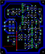
I don't have the time right now but I'll put a stereo potentiometer at the left side and I'll put the power connectors to the right side hoping to avoid the jumper wire...
Maybe integrating a regulated power supply is a good idea ??
Maybe integrating a regulated power supply is a good idea ??
I guess that this design of PCB is not good and will bring problems with hum, 'cos ground loop is closed. It must be interrupted and ground of both channels must lead to the middle of PS separately.
pjacobi said:Don't know about the other points raised, but circuit as shown can swing +-12V. Putting the upper cascode higher will reduce swing.
Data for JFET mod is comparable, and you get higher swing for lower VTO.
Seems like I must correct myself here, you are right. Actually that 47k is not the base stopper… 🙄 (I put it now into the spice and have seen the negative half clipping at about 8.5V.) And JFET applied directly without biasing network did not limit the swing (as I expected).
However, I would rather like to see a higher Vce, even if it is supposed to be held constant.
tcpip said:I find your comments interesting, and want to see what you mean, but I can't follow the terms you use... I have almost no knowledge of circuit design. Can you please repeat your comments and include actual references to things like R9 and C10 in my schematic? Please? Just repeat it all for just one channel, and I'll follow your suggestions to see what you're talking about.
According to the things just said, here is the slightly corrected idea.
Principally, if you raise the impedance seen by C10, you might reduce its value which enables possibility to use a better cap. In this concrete situation this impedance is mainly formed by R13+(R14//R15), so you could raise it raising R13’s value. This resistance, seen by the Q5’s base current (which is equal to Ic/hFE of the used piece), will however, when raised, develop more voltage across it and this will additionally alter the DC points of the cascode set by the resistor network (R14/R15), namely the voltages of the cascoding device will go lower thus further reducing Vce of the pass transistor, so this must be taken into account.
Another way is to leave that R13 as it is, and to raise the values of R14 and R15.
And another way is to go only with one resistor (R13) referred to the positive supply. Here you should really know Q5’s base current.
Note also that too high impedance seen by the base is often considered as not very welcome.
Hope this helps rather than confuses.
Pedja
Ouch. I didn't know this would be the case even in low power circuits like this one. Jean-Paul, any comments? I'd think hum wouldn't even reach the PCB (assuming it's mains hum you're talking about) because a regulated PSU would bring down all ups and downs to somethign like a few uV, won't it?Upupa Epops said:I guess that this design of PCB is not good and will bring problems with hum, 'cos ground loop is closed. It must be interrupted and ground of both channels must lead to the middle of PS separately.
Tarun
jean-paul said:I don't have the time right now but I'll put a stereo potentiometer at the left side and I'll put the power connectors to the right side hoping to avoid the jumper wire...
I thought about the avoiding of the jumper, but I can't see how I'll achieve that, because wherever I put the supply terminals, the positive line has to reach both upper and lower extremes of the board. Now I'm wondering whether it would have been a better idea to make a broad and short board with the left and right channels one beside the other instead of one below the other. That way, the supply lines could have been long horizontal tracks moving from left to right on the upper and lower edges of the board. Maybe someday I'll do another board like that. 🙂
I thought about it, but I felt that I'll often need more than one buffer in a chassis, so I might as well keep the two separate.Maybe integrating a regulated power supply is a good idea ??
Tarun
Thanks for the trouble. I haven't yet sat down with your comments and the circuit; I'll do it soon. I won't understand the deeper reasoning behind your suggestions, but I'll at least understand the current flow changes you've described. Thanks again. 🙂Pedja said:Note also that too high impedance seen by the base is often considered as not very welcome.
Hope this helps rather than confuses.
Tarun
Some general doubts about layout and component placement
Ok, here are some general questions:
Tarun
Ok, here are some general questions:
- Why don't any PCBs I see have vertically mounted resistors? I'm talking audio frequencies, not frequencies where every wire acts like an antenna. Won't vertical resistors save a lot of space?
- What are your thoughts about how to do layout ground tracks for audio preamp-type circuits? Is a star ground needed? Is it necessary to keep signal ground separate from supply ground? Which of the following do you do?
(i) Keep the two totally separate; join them outside the board at some star ground point
(ii) Keep them separate for the entire board, except at one "star" point where you join them (that's what I've done in the board above)
(iii) join them freely wherever you feel like, because the magnitudes of current flowing through these tracks is so minor anyway. - When you take shielded hookup wire from PCB to pots/switches, where do you ground the shield? Do you make a ground solder-pad on the PCB for the shield of each such cable? If not, what else?
Tarun
Re: Some general doubts about layout and component placement
This was my comment too on the original board and I will change that. In real life it will not give too much problems I think. Nevertheless it can be done better and it will be changed.
But what about downloading the files and making a perfect PCB ?? Show us you're the masta !
A ground loop has enough with a few mV, even a regulated supply can't help. Star grounds are preferred.
Discussing ground-design will be a never ending discussion. I have a very old guide dating from the tube era with the correct information and when I started to do things as described I haven't had any hum problems since. Ground issues alone are enough for a new thread 😉
I found one selfmade version of the original boards and it has the resistors standing up. I added decoupling caps and pcb tracks for ground. Never liked resistors mounted standing up but I really don't see technical drawbacks for doing so. The reason to mount them horizontally was the lower inductance of the lead wires but when I dismantle a tuner I see resistors standing up so this is not a too stringent "law".
Upupa Epops said:I guess that this design of PCB is not good and will bring problems with hum, 'cos ground loop is closed. It must be interrupted and ground of both channels must lead to the middle of PS separately.
This was my comment too on the original board and I will change that. In real life it will not give too much problems I think. Nevertheless it can be done better and it will be changed.
But what about downloading the files and making a perfect PCB ?? Show us you're the masta !
Originally posted by tcpip Ouch. I didn't know this would be the case even in low power circuits like this one. Jean-Paul, any comments? I'd think hum wouldn't even reach the PCB (assuming it's mains hum you're talking about) because a regulated PSU would bring down all ups and downs to something like a few uV, won't it?
Tarun
A ground loop has enough with a few mV, even a regulated supply can't help. Star grounds are preferred.
Discussing ground-design will be a never ending discussion. I have a very old guide dating from the tube era with the correct information and when I started to do things as described I haven't had any hum problems since. Ground issues alone are enough for a new thread 😉
I found one selfmade version of the original boards and it has the resistors standing up. I added decoupling caps and pcb tracks for ground. Never liked resistors mounted standing up but I really don't see technical drawbacks for doing so. The reason to mount them horizontally was the lower inductance of the lead wires but when I dismantle a tuner I see resistors standing up so this is not a too stringent "law".
Re: Re: Some general doubts about layout and component placement
If star grounding is the thing to aim for, is it okay to take ground tracks from one edge to another using jumpers? Sometimes I don't see any way out but to do that, if I have to do star-grounding.
Tarun
Wow. Angshu too seems to follow star grounding for signal-level PCBs, but I'd asked Randy (Slone) once, and he'd said that it's not a critical issue for low-current PCBs. Of course, I haven't seen any Randy Slone PCB layout with the ground track going full circle like mine, so I can't say he'd have approved my current design. 🙂 However, the key things that he'd explicitly told me werejean-paul said:A ground loop has enough with a few mV, even a regulated supply can't help. Star grounds are preferred.
- I don't have to separate supply ground and signal ground in such PCBs.
- I don't have to aim for star grounding.... a long ground track with connections to various components at various places is adequate.
If star grounding is the thing to aim for, is it okay to take ground tracks from one edge to another using jumpers? Sometimes I don't see any way out but to do that, if I have to do star-grounding.
Tarun
PCB rules
Hi TCPIP,
In general there not a secret rule when you disigern the pcb, only
depend of your desisgner.
The best PCB is not PCB for questions of dialectric,
If you have a compromise of the rule for me the best substrat is teflon
yes it is very expensive but it has the best perfmans .
By Carefully in the grounds in your designer becouse the grounds you have the same tratement or mor the the live line.
Please check: pcbcafe.com
or EMC and the Printed Circuit Board (Mark I . Montrose)
Printed Circuit Board Design Techniques for EMC compliiance.
If I´ll can help you for your PCB , contant whit me
Jesús Puerto
- Status
- Not open for further replies.
- Home
- Source & Line
- Analog Line Level
- Simple discrete unity gain buffer