.... The behavior is like parabola.
You have to locate its focus! 😆
Sorry, I couldn't resist.
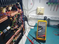
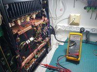
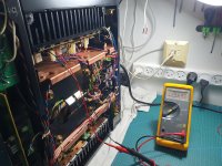
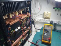
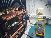
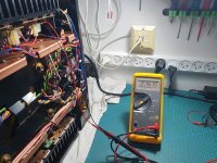
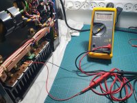
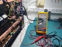
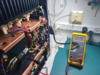
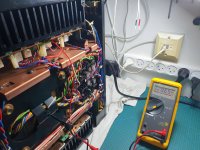
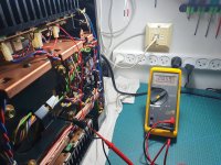
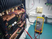
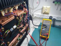
I connected a meter to forklike FET output and the voltage is even not close to the bias voltage. Bias voltage is 26mV and on the 8 point there's +/- 2V. This is the 8 output voltage of the right channel on the forklike. The test was on all the outputs on the 2 sides as the last pic
Attachments
-
 20250109_212941.jpg609.5 KB · Views: 38
 -
 Screenshot_20250109_214526_Gallery.jpg221.4 KB · Views: 47
 -
 20250109_213700.jpg621.3 KB · Views: 41
 -
 20250109_213637.jpg567.5 KB · Views: 38
 -
 20250109_213616.jpg587.3 KB · Views: 35
 -
 20250109_213539.jpg584.9 KB · Views: 35
 -
 20250109_213454.jpg601.3 KB · Views: 36
 -
 20250109_213429.jpg589.4 KB · Views: 35
 -
 20250109_213007.jpg648.3 KB · Views: 35
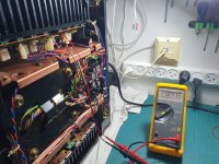
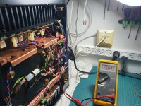
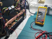
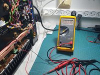
And this is the left channel. 1.5V and 1.7V while on right channel there's 2.1V and 1.9V
Attachments
-
 20250109_214705.jpg699.5 KB · Views: 24
 -
 20250109_214740.jpg692.5 KB · Views: 25
 -
 20250109_214817.jpg699.9 KB · Views: 25
 -
 20250109_214851.jpg708.2 KB · Views: 22
 -
 20250109_214915.jpg675.7 KB · Views: 23
 -
 20250109_214938.jpg624.3 KB · Views: 26
 -
 20250109_215002.jpg651 KB · Views: 23
 -
 20250109_215021.jpg650.3 KB · Views: 25
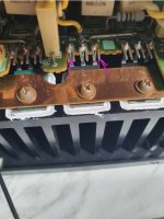
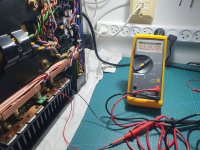
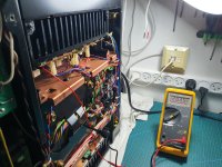
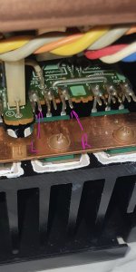
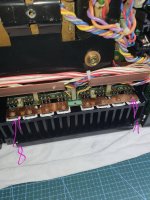
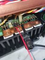
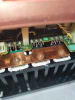
Black clip to channel output = speaker output of each of the 4 channels and then measure each fork with red tip.
Look, each channel has 4 transistors and in the middle between 2 left and 2 right transistors is speaker output.
Alternatively you could hook black to ground but reading will be falsified by output offset voltage.
In the picture one output is labeled A on the left side of the pcb, you measure 12 forks of surrounding transistors against that.
Same for the right side where output is labeled C.
You will get 26mV bias , rail voltage and gate voltage on each transistor.
We are interested in the bias.
Last edited:
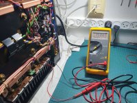
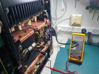
Right channel with the middle output refer to the ground. There is 28V
Attachments
-
 20250109_221032.jpg537.9 KB · Views: 31
 -
 20250109_221023.jpg586.6 KB · Views: 35
 -
 20250109_221012.jpg574.3 KB · Views: 24
 -
 20250109_220959.jpg593.2 KB · Views: 28
 -
 20250109_220942.jpg574.1 KB · Views: 29
 -
 20250109_220923.jpg617.3 KB · Views: 28
 -
 20250109_220850.jpg620.9 KB · Views: 27
 -
 20250109_220832.jpg636.4 KB · Views: 27
no. Please read again post 46 and 47, I editedOk. So one leg of the meter to the middle output of the transistor and the other leg to ground?
Same voltage on the right. The only thing that I see is that on the left channel there's 1.5V and 1.7V between the 2 sides output transistors and on right there's 2.1 and 1.7V much higher and that's why the right channel is much hotter.
Yes, middle is drain of the FET and that is about + / - 29VRight channel with the middle output refer to the ground. There is 28V
But we need the left or the right fork of the FET.
Now please instead of the middle fork to ground measure the left and right forks of each FET to ground
Left channel:
Tran. #1 R - 1.58V L (-55)-(50)mV jumpy
Tran. #2 R - 1.59V L (-45)-(60)mV jumpy
Tran. #3 R +1.8V L 50-120mV jumpy
Tran. #4 R +1.85V L 74-110mV jumpy
Tran. #5 R +1.65V L (-18)-(45)mV jumpy
Tran. #6 R +1.57V L (-65)-(5)mV jumpy
Tran. #7 R - 1.83V L (-152)-(-82)mV jumpy
Tran. #8 R - 1.87V L (-90)-(-30)mV jumpy
I don't know why it act like that
Attachments
Ok, looks like something wrong Tran 6
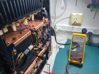
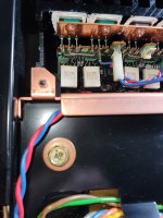
Please repeat like in the picture: Black clip on the pin on the pcb.
Only measure L for each transistor. R not need.

Please repeat like in the picture: Black clip on the pin on the pcb.
Only measure L for each transistor. R not need.
Right channel:
Tran. #1 R -1.88V L 50-100mV jumpy
Tran. #2 R -1.84V L 55-110mV jumpy
Tran. #3 R 1.86V L 65-134mV jumpy
Tran. #4 R 1.84V L 91-132mV jumpy
Tran. #5 R 2V L 182-210mV jumpy
Tran. #6 R 2V L 68-148mV jumpy
Tran. #7 R -2.13V L 15-38mV jumpy
Tran. #8 R -2V L 43-64mV jumpy
Tran. #1 R -1.88V L 50-100mV jumpy
Tran. #2 R -1.84V L 55-110mV jumpy
Tran. #3 R 1.86V L 65-134mV jumpy
Tran. #4 R 1.84V L 91-132mV jumpy
Tran. #5 R 2V L 182-210mV jumpy
Tran. #6 R 2V L 68-148mV jumpy
Tran. #7 R -2.13V L 15-38mV jumpy
Tran. #8 R -2V L 43-64mV jumpy
Attachments

I don't understand.To check all the Transistors with the cold pin or also with the hot?
edit: both, see next post.
Last edited:
Please do with left channel like I drawn in post #54
Attach the black clip to the C pin in the left area of the pcb and measure the 4 L, then move the black clip to the C pin in the right area and measure the 4 L there.
Attach the black clip to the C pin in the left area of the pcb and measure the 4 L, then move the black clip to the C pin in the right area and measure the 4 L there.
Did you still measure to ground here ?Right channel:
Tran. #1 R -1.88V L 50-100mV jumpy
Tran. #2 R -1.84V L 55-110mV jumpy
Tran. #3 R 1.86V L 65-134mV jumpy
Tran. #4 R 1.84V L 91-132mV jumpy
Tran. #5 R 2V L 182-210mV jumpy
Tran. #6 R 2V L 68-148mV jumpy
Tran. #7 R -2.13V L 15-38mV jumpy
Tran. #8 R -2V L 43-64mV jumpy
- Home
- Amplifiers
- Solid State
- Sansui Alpha AU-907i MOS Limited