Models:
standard.jft
.model 2sk170 NJF(Beta=71.86m Rs=4.151 Rd=4.151 Betatce=-.5 Lambda=1.923m Vto=-.4124 Vtotc=-2.5m Cgd=20p M=.3805 Pb=.4746 Fc=.5 Cgs=25.48p Isr=84.77p Nr=2
Is=8.477p N=1 Xti=3 Alpha=10u Vk=100 Kf=111.3E-18 Af=1)
standard.bjt
.MODEL mjl3281a npn IS=9.8145e-12 BF=438.0 NF=1.00 VAF=38 IKF=19.0 ISE=1.0e-12 NE=1.1237388682 BR=4.98985 NR=1.09511 VAR=4.32026 IKR=4.37516
ISC=3.25e-13 NC=3.96875 RB=3.997 RE=0.00 RC=0.06 XTB=0.115253 XTI=1.03146 EG=1.11986 CJE=1.144e-08 VJE=0.468574 MJE=0.34957 TF=2.6769e-9 XTF=7500
VTF=3.0 ITF=1000 CJC=1.093685e-9 VJC=0.623643 MJC=0.482111 XCJC=0.959922 FC=0.1 CJS=0 VJS=0.75 MJS=0.5 TR=1e-07 PTF=0 KF=0 AF=1 Vceo=200 Icrating=15
mfg=OnSemiconductor
.MODEL mjl1302a pnp IS=9.8145e-12 BF=122.925 NF=1.00 VAF=40 IKF=19 ISE=9.18577762370362E-07 NE=5.0 BR=4.98985 NR=1.09511 VAR=4.32026 IKR=4.37516
ISC=3.25e-13 NC=3.96875 RB=3.30 RE=0.00 RC=0.06 XTB=0.115253 XTI=1.03146 EG=1.11986 CJE=1.561e-08 VJE=0.781803 MJE=0.433868 TF=3.257e-9 XTF=1000
VTF=2.0 ITF=260 CJC=2.346838e-9 VJC=0.27876 MJC=0.411324 XCJC=0.959922 FC=0.1 CJS=0 VJS=0.75 MJS=0.5 TR=1e-07 PTF=0 KF=0 AF=1 Vceo=200 Icrating=15
mfg=OnSemiconductor
.MODEL Qmje15031 pnp(IS=7.17489e-11 BF=457.169 NF=1.11376 VAF=6.01557 IKF=0.345808 ISE=1e-08 NE=2.18567 BR=0.247882 NR=1.39549 VAR=60.1557
IKR=0.0263893 ISC=1e-16 NC=2.89486 RB=2.29208 IRB=0.0114006 RBM=0.000102795 RE=0.00815557 RC=0.0407779 XTB=0.1 XTI=0.1 EG=1.05 CJE=1.64037e-09
VJE=0.819491 MJE=0.537987 TF=1.60991e-09 XTF=180.82 VTF=1.16561 ITF=6.50499 CJC=4.82516e-10 VJC=0.4 MJC=0.374287 XCJC=0.786653 FC=0.712788 CJS=0
VJS=0.75 MJS=0.5 TR=3.32795e-08 PTF=0 KF=0 AF=1)
.MODEL Qmje15030 npn(IS=3.894e-11 BF=312.524 NF=1.0979 VAF=9.9963 IKF=0.796201 ISE=2.37397e-09 NE=1.94897 BR=0.14246 NR=1.64791 VAR=99.9749
IKR=0.00539895 ISC=2.33175e-09 NC=2.79024 RB=267.202 IRB=9.99994e-13 RBM=0.299835 RE=3.04316e-05 RC=0.252928 XTB=0.1 XTI=3.92812 EG=1.05
CJE=2.42998e-09 VJE=0.794171 MJE=0.569313 TF=1.87986e-09 XTF=1000 VTF=1835.34 ITF=270.188 CJC=2.43127e-10 VJC=0.4 MJC=0.361453 XCJC=0.802892 FC=0.8
CJS=0 VJS=0.75 MJS=0.5 TR=9.86194e-06 PTF=0 KF=0 AF=1)
.MODEL 2SC3423 NPN(IS=9.98627F BF=2K NF=967.67M VAF=100 IKF=49.6929M ISE=1.04163F NE=1.07574 BR=601.257M IKR=462.798U ISC=32.904P RC=899.97M
CJE=2P MJE=500M CJC=6.42174P VJC=749.999M MJC=499.509M TF=713.346P XTF=500M VTF=10 ITF=9.9976M TR=10N)
.MODEL 2SA1360 PNP(IS=10F BF=134.853 VAF=100 IKF=109.96M ISE=221.874F NE=1.66575 BR=10 IKR=880.176M ISC=187.58P NC=1.90472 RE=1 RC=15.5104
CJE=2P MJE=500M CJC=6.24728P VJC=692.028M MJC=340.013M TF=1.08385N XTF=16.9293 VTF=9.36211 ITF=670.025M TR=10N)
.model BC560C PNP(Is=1.02f Xti=3 Eg=1.11 Vaf=34.62 Bf=401.6 Ise=38.26p Ne=5.635 Ikf=74.73m Nk=.512 Xtb=1.5 Br=9.011 Isc=1.517f Nc=1.831 Ikr=.1469 Rc=1.151
Cjc=9.81p Mjc=.332 Vjc=.4865 Fc=.5 Cje=30p Mje=.3333 Vje=.5 Tr=10n Tf=524p Itf=.9847 Xtf=17.71 Vtf=10)
.MODEL BC550C NPN (LEVEL=1 IS=2.24183E-14 NF=0.996496 ISE=1.90217E-14 NE=2 BF=228.4 IKF=0.211766 VAF=161.939 NR=0.993 ISC=4.7863E-15 NC=0.996
BR=12.1807 IKR=0.3423 VAR=123.229 RB=167.033 IRB=7.079458E-05 RBM=1.12256 RE=0.036 RC=0.79 XTB=1.65 EG=1.1737 XTI=3 CJE=1.87E-11 VJE=0.732 MJE=0.33
CJC=6.16E-12 VJC=0.395 MJC=0.251 XCJC=0.6192 FC=0.5 TF=518.15E-12 XTF=10 VTF=10 ITF=1 TR=10.000E-9)
standard.dio
.model Dnjl0302 D(IS=5.17122e-08 RS=0.0324668 N=1.78236 EG=1.12011 XTI=0.5 BV=200 IBV=2e-06 CJO=5.59229e-11 VJ=0.4 M=0.346657 FC=0.5 TT=2.59685e-08
KF=0 AF=1)
.model Dnjl0281 D(IS=5.17122e-08 RS=0.0324668 N=1.78236 EG=1.12011 XTI=0.5 BV=200 IBV=2e-06 CJO=5.59229e-11 VJ=0.4 M=0.346657 FC=0.5 TT=2.59685e-08
KF=0 AF=1)
.model Rled D(Is=.27n Rs=5.65 N=3.95 Cjo=42p Iave=30m Vpk=5 mfg=Nichia type=LED)
.model Gled D(Is=1e-22 Rs=6 N=1.7 Cjo=50p Iave=160m Vpk=5 mfg=Fairchild type=LED)

Sheldon said:.. is there a significant advantage to dual front end supplies for this design?
Sheldon
Hi Sheldon,
Yes, there are two main reasons for an dedicated input stage PSU:
- PSRR. Cascode devices bases are conected to rayls, so a very quiet supply is needed.
- Limited headroom because of cascode topology - waste of output stage potential power.
The only disadvantage is a slow recovery from output stage clipping, but in my case the amp will never clip because I have a DAC in the same case with the power amp and there is no analog input. The zero digital of DAC provide an max input voltage which don't drive to clipping the power amplifier
Mihai
Hello all,
After a quick cross-reading ( new word ? 😎 ) of the first pages, I've found interesting facts about amplifier, well. But, never something which talk about transformers
except the fact you hate common industrial transformers.
So, I'll start to think about it.
Two stages who need separated supplies. Preamp and power one.
Preamp need symetrical 39 V and power only 34V and your PSU schematic don't answer to my question.
Is something like 300 VA / channel for power and 25 VA / channel for preamp is good ?
Thanks you
roender said:
Hi Sheldon,
Yes, there are two main reasons for an dedicated input stage PSU:
- PSRR. Cascode devices bases are conected to rayls, so a very quiet supply is needed.
- Limited headroom because of cascode topology - waste of output stage potential power.
The only disadvantage is a slow recovery from output stage clipping, but in my case the amp will never clip because I have a DAC in the same case with the power amp and there is no analog input. The zero digital of DAC provide an max input voltage which don't drive to clipping the power amplifier
Mihai
Ahh,
Sorry Mihai, I didn't make my question clear. In your case I see what looks like two separate main supplies and also two separate input supplies. I was curious as to whether you would expect a audible difference between a stereo amp with a single input supply for both channels vs separate input supplies for each channel - a separate output power supply assumed for either case. As the power demand for the input section is low and fairly constant, I would think that the intermodulation between channels might be low enough to ignore.
Sheldon
i'am asking samething than Sheldon. And If a big 500VA with separate rectifiers can be good, i'm short in space in my case. 
Sheldon said:
I would think that the intermodulation between channels might be low enough to ignore.
Sheldon
Maybe, I don't know.
You could try first with a single PSU and see how it works and if you are not satisfied then build a second frontend PSU.
DRZ1 said:i'am asking samething than Sheldon. And If a big 500VA with separate rectifiers can be good, i'm short in space in my case.
Denis,
Try and see how well it will work. Don't forget to double the filtering capacitors if you use a single power PSU, at least 40mF per rail.
Mihai
DRZ1 said:i'am asking samething than Sheldon. And If a big 500VA with separate rectifiers can be good, i'm short in space in my case.
I haven't done any careful listening tests on this issue with solid state amps, though I have done monoblocks and stereo amps with a shared transformer and separate rectifiers. My experience with class A tube amps is that I cannot perceive any sonic benefit to separate supplies for each channel. I have to add the caveat that most of my testing is with a multiamped system. If I spent more time listening to single amped systems, maybe I'd hear differences.
Sheldon
Hi,
My experience with this is that a single supply with separate regulators for the voltage amp stage will do everything you need. The output stage can use a shared supply with the other channel, or separate rectifiers and filters. The voltage gain in most output stages is close to unity. Even if there is some gain, the error correction stage is isolated and will reduce any cross talk.
-Chris
Well, i agree with you guys, the cross talk comes from the low level section.
I think that the config of this amp permit a single transfo with separate bridges and filtration for the power section, at condition that the reserve in the filtration is big enough, 4 X 10000uF per side seems to be OK and the power reserve of the transfo is big too for good regulation.
I'm in the way to use single transfo for the power stage and another one for the front stage. Each side will have their own rectifier and filtration (regulator in the case of front stage).
Roender,
Interesting original design. I have a few questions and I am sorry if they have been already answered (it is a long thread....).
1) Since it is a bjt output stage why is there no overcurrent protection circuit like most of power amp with bjt output stage? Is the thermal track temperature behavior enough?
2) For the jfet transistors, can you specify the recommended or optimum IDSS current for the used device (best THD/noise compromise).
3) an amp gain of 45 is a little bit high. A lot of "power amps" have more like 20 of gain. If someone wants to use gain of 20 (because use of separate pre-amp with gain or other reason), what would be the components changes so the amp keeps its characteristics as your original design (gain bandwidth, stability, ...)?
4) do you think bypassing C21 (470uf feedback cap) with 100nf metal film or else type would worth it? are you sure about the indicated orientation of the polarity (+)? what about non-polarysed type for electrolytic?
Thanks
fab said:
1) Since it is a bjt output stage why is there no overcurrent protection circuit like most of power amp with bjt output stage?
2) ... specify the recommended or optimum IDSS current for the used device (best THD/noise compromise).
3) If someone wants to use gain of 20 (because use of separate pre-amp with gain or other reason), what would be the components changes so the amp keeps its characteristics as your original design (gain bandwidth, stability, ...)?
4) do you think bypassing C21 (470uf feedback cap) with 100nf metal film or else type would worth it? are you sure about the indicated orientation of the polarity (+)? what about non-polarysed type for electrolytic?
Thanks
Hi Fab,
1. The SOA of output stage is so high for used rail voltage that there is no need for an active overcurrent protection. A simple output shunt DC protection will protect speakers and output transistors if fuses are no higher than T4A.
2. The optimum Ids current for 2sk170BL is as much as it take, very close to BL max limit, or even better use a V grade.
3. I like to have a very high CL gain in order to minimize error signal range in LTP. I don't like the idea of an preamp with gain.
If someone want to modify this design for other CL gain, he/she must do the math and listening tests for the modified compensation network.
4. There is no need to bypass a low ESR capacitor. If you use a "normal" cap you could try to bypass it with a very good film capacitor.
The DC component over the feedback capacitor is almost zero, if you have a JFET LTP, so doesn't meter how that cap is mounted.
Mihai
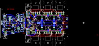
Here's my latest layout.
Due to the size and orientation of my heatsinks, I have to remove the big filter caps from the amp board. Also, I left more room for C21.
Mihai, or anyone else, please let me know if you see anything wrong.
I'm not sure if I make PCB myself, or I send it out to have the board made professionally.
Due to the size and orientation of my heatsinks, I have to remove the big filter caps from the amp board. Also, I left more room for C21.
Mihai, or anyone else, please let me know if you see anything wrong.
I'm not sure if I make PCB myself, or I send it out to have the board made professionally.
Attachments
Niner
From electrically point of view looks good but aesthetically is ugly 😀
Go ahead and see how it work.
Mihai
From electrically point of view looks good but aesthetically is ugly 😀
Go ahead and see how it work.
Mihai
I know, Mihai. I'm messing with your beautiful child 😀
I probably will make the PCB at home. I was quoted ~$100 for two amp boards.
I probably will make the PCB at home. I was quoted ~$100 for two amp boards.
Can this design be easily adapted for Lateral mosfet in place of thermal track bjt for output stage?
what would be the pros and cons?
Thanks
what would be the pros and cons?
Thanks
Transistor type?
Hi Roender
According to your schematics disclosed in post #8, why Q15 and Q10 are medium power transistors and not simply to-92 type?
There should be only about 2ma passing through thus about 70mW or so ...
Thanks
Hi Roender
According to your schematics disclosed in post #8, why Q15 and Q10 are medium power transistors and not simply to-92 type?
There should be only about 2ma passing through thus about 70mW or so ...
Thanks
- Home
- Amplifiers
- Solid State
- RMI-FC100, a single stage audio power amplifier