I have done further experiments with IIC and TPIIC, and I was able to get good stability with a 6 dB increase in loop gain between 2 kHz and 20 kHz. However, it had no effect on distortion. All significant distortion in this amp seems to be in the output stage. IIMC specifically excludes the output stage. That also confirms that the folded cascode input/VAS stage contributes almost nothing to the amp's THD.
A few posts back, I looked at the effect of input RE degeneration, and found that lower RE gave lower amplifier THD. However, lower RE boosts the Gm of the input pair, requiring a proportional increase in the compensation caps, thus lowering slew rate. What I need is a way to increase the gain that does not require an increase in the compensation caps. By accident, that is what happened next.
I looked at increasing the bias current of the pre-driver stage. Increasing it makes distortion go up, not down. So, I tried decreasing it, instead.
The sweet spot for pre-driver bias seems to be around 1/2 the current I was running before, so about 3.8mA in the pre-driver.
Ibias ---- THD <1kHz ---- THD 20kHz
7.5mA --- 0.00045% ----- 0.00163
2.8mA --- 0.00028% ----- 0.00150
In the schematic this changes R12 and R13 from 249 to 475. The folded cascode input/VAS is looking close to final form.
My intuition was that increasing current would increase the linearity of loading on the VAS. I was wrong. The loading is already quite linear. Pre-driver current is fairly constant vs signal swing. The pre-driver adds linearity to the VAS, but more importantly, it adds gain to the VAS. The increased loop gain corrects output stage distortion.
Next, I will look at optimizing the driver stage to reduce THD. When I changed out the KSC2690/KSA1220 for multiple KSC3503/KSA1381, distortion went up significantly at low frequency, but down at high freq. I will check THD vs driver-stage current. I do not have any intuition about whether the driver bias current is too high or too low. Perhaps some other circuit change would help.
The output transistors are pretty well optimized wrt Oliver effect, but I'll re-examine that, too.
Last edited:
The key thing I have learned today is that a folded cascode input/VAS stage has almost zero non-linearity, relative to the output stage. This is not mentioned in any literature I have seen. (I'm sure Scott Wurcer knows it, however.)
Hi Russell: really nice work that you have done so far (including the biasing and SOA sub circuits).
Have you considered some form of error correction in the output stage?
Along the lines of the following, for example:
http://www.diyaudio.com/forums/atta...7d1237669327-genesis-stealth-amp-gstealth.gif
Alternatively, using the above schematic as a starting point, if you don't mind adding a separate low-power class A output stage, it should be possible to tie the bases/gates of the existing Class AB output devices to the same nodes as the differential amplifier inputs, connect the inputs of the small class A output stage to the differential amp outputs, and sum the outputs of the big class AB output stage and the small Class A output stage through a summing network.
Conceptually this would be similar to what Sansui did with their Feed-Forward Correction power amplifiers from the early 1980s.
Thanks. I appreciate the kudos. I mostly know what I'm doing, and I'm doing experiments to fill in what I don't know.
Earlier today, I was thinking, maybe I could find some form of error correction for the output stage. The circuit you show is rather like a CFP, but with diff-amps replacing the complementary devices. I actually have built a circuit like that around MOSFETs, to boost Gm*ro of the device, but it was the folded cascode transistors of a CMOS headphone IC. That HPA had an open-loop gain of over 160 dB. We wanted all that gain to correct output stage nonlinearity (just like here).
That sort of thing may be just the ticket here. It would have to have a very high BW to work. For now, I'm going to see how much I can optimize the output stage just by setting bias current levels. The distortion is already close to my design goals. Mostly, I don't want to leave any performance on the table with the topology and parts I already have in place.
I read the thread whence that schematic came. I felt really bad for OStripper. That Genesis amp is a beast.
I think he got the schematic wrong by putting diodes at the input. They would turn the MOSFET outputs into constant 3A current sources, which would not want to drive the load. The Genesis amp sets that spread with a resistor. That resistor is between complementary emitters of a class-A amp that drives the input of the circuit you linked. At frequencies where the "booster" diff-amps crap out, a feedforward cap bypasses the diff-amps, and connects the class-A output directly to the MOSFET gates. There is no global feedback at all, so the designer only had to worry about stabilizing the local loops.
Every. Single. MOSFET. gets it's own diff-amp booster. Someone did not want to spend time matching MOSFETs.
That VAS circuit is the most wacked thing I have seen. A transformer couples the input amps to the VAS, and the transformer secondaries feed straight into the emitters of complementary common-base amplifiers. The transformer input is held at zero volts DC by an adapted CMFB circuit.
I'm looking at the Genesis amp here:
https://audio-circuit.dk/wp-content/uploads/simple-file-list/genesis/Genesis-B200Stelth-pwr-sch.pdf
Thank you for showing me that circuit.
Got hooked
I certainly want to follow the project and build your amp, Russell.
There are a few things about your amp that got me hooked, those that I wanted to try but do not have the level of the design skills like yours to implement.
Years ago when I was constructing a 200W amp, I attempted but then gave up on a Diamond 3EF output stage using On-semi ThermalTrak power transistors, as I couldn't put together a satisfactory bias control scheme that would incorporate the internal diodes of the ThermalTrak transistors and would arrive at a bias voltage just a smidgen over 1V across the pre-driver transistors' base. I ended up settling at a "normal" 3EF output stage. I have been since happily enjoying that amp for almost 6 years and forgot about the diamond 3EF. Your project reignited me.
The transimpedance VAS, or lack of a VAS, is a gain topology I had remotely in mind too, yet never have come up with an amp as a vehicle.
I like the way you split-compound the driver transistors into the output transistors making them super fast.
I like the way you "abuse" the TLV431 to stop the SOA protection transistors creeping on. Clever.
Your fix to William Chater's bias servo actually makes William's dream come true. I was like "son of a b...." when I saw you sense the drop from the rails and scale them into a current summer. Just brilliant! The simulated performance is very convincing. It should obsolete the ThermalTrak devices altogether if I may say so, and relief much of the pain in the amp design with regard to thermal related bias stability.
The SLABS, that makes the SOA limit protection and the bias servo into one sub-module, is a great idea. By making it a sub module it hops out of the confinement of RK-Auto200W amp, and opens itself up to most all power amp designs, and any one can try it. I think you might want to consider recommend SLABS to Ostriper's on-going Wolverine DiyA store amp development. I like your SLAB idea so much that I couldn't resist myself, and had a go in KiCAD to see what I could come up with. Turns out it can be laid out within a 2"X2" PCB (with 0805 size passive parts in stead of 1206).

Very much appreciate you bringing in the great ideas and brilliant designs, in one integrated project.
I certainly want to follow the project and build your amp, Russell.
There are a few things about your amp that got me hooked, those that I wanted to try but do not have the level of the design skills like yours to implement.
Years ago when I was constructing a 200W amp, I attempted but then gave up on a Diamond 3EF output stage using On-semi ThermalTrak power transistors, as I couldn't put together a satisfactory bias control scheme that would incorporate the internal diodes of the ThermalTrak transistors and would arrive at a bias voltage just a smidgen over 1V across the pre-driver transistors' base. I ended up settling at a "normal" 3EF output stage. I have been since happily enjoying that amp for almost 6 years and forgot about the diamond 3EF. Your project reignited me.
The transimpedance VAS, or lack of a VAS, is a gain topology I had remotely in mind too, yet never have come up with an amp as a vehicle.
I like the way you split-compound the driver transistors into the output transistors making them super fast.
I like the way you "abuse" the TLV431 to stop the SOA protection transistors creeping on. Clever.
Your fix to William Chater's bias servo actually makes William's dream come true. I was like "son of a b...." when I saw you sense the drop from the rails and scale them into a current summer. Just brilliant! The simulated performance is very convincing. It should obsolete the ThermalTrak devices altogether if I may say so, and relief much of the pain in the amp design with regard to thermal related bias stability.
The SLABS, that makes the SOA limit protection and the bias servo into one sub-module, is a great idea. By making it a sub module it hops out of the confinement of RK-Auto200W amp, and opens itself up to most all power amp designs, and any one can try it. I think you might want to consider recommend SLABS to Ostriper's on-going Wolverine DiyA store amp development. I like your SLAB idea so much that I couldn't resist myself, and had a go in KiCAD to see what I could come up with. Turns out it can be laid out within a 2"X2" PCB (with 0805 size passive parts in stead of 1206).
Very much appreciate you bringing in the great ideas and brilliant designs, in one integrated project.
Thanks, nattawa. I really appreciate the glowing review.
I first saw a folded cascode (FC) VAS stage in a review of Jeff Rowland's Model 7 amplifier in 1990. I was stunned that differential input, all the gain and voltage swing could be attained in a single-stage. I first designed one into a production amp 11 years later, but there were still some aspects of its compensation that I did not understand. Ironically, I did not know about Scott Wurcer's AD797 design until about 5 years ago.
In 2001, I moved from designing discrete transistor amps to designing analog integrated circuits. In IC design, FC is the dominant topology. I've designed quite a number of them, now, usually as building blocks in larger systems.
Thanks for noticing that SLABS is portable. You do have to put in the 0.1 ohm sense resistors, and figure out how to adapt the servo current to your own biasing. It is set up for adjusting a PNP current source in the VAS stage.
I've been out of the discrete transistor power amp game for two decades now, but in the meantime, I've had lots of ideas. I also have some ideas for making a better class-D amp. I even have a patent for a circuit that auto-zeroes the deadtime of a class-D output stage.
Nattawa,
One thing I want to add.
I think it's very cool that you did a PCB for the SLABS. I hate to mess up the 2" x 2" PCB, but I should mention that Q11 and Q12 dissipate around 1W each. They need to be TO-220 TIP35C/36C with heat sinks attached.
Be sure to check the dissipation of the 0805 resistors, too. A quick glance says they look OK.
Thanks, Russell. I did go through the resistor dissipation and they checked out. I was indeed unsure of the dissipation of Q11/12. I'll try if I can have Q11/12 go on a heatsink mounted to the four mounting holes, on the back side of the PCB, as a way of retaining the 2x2 size.
I found the magic option in this particular circuit to make it run almost every time.
.options cshunt 0.1p
If all you're trying to do is to nudge the simulator to converge, you can probably reduce that a bit. 1 fF would probably be plenty. Though 100 fF (or 0.1 pF if you prefer) is not completely unreasonable, especially if you're using a ground plane.
Similarly rshunt = 1e12 or gshunt = 1e-12 can help if the simulator supports it. That adds a resistance (or conductance, respectively) from each node to ground.
Tom
An imperious doodling indeed - I will need to take a long breath to examine it in detail.
I'll need to breathe pure oxygen.
Somebody spent a lot of time thinking on this. 😀
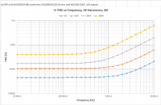
Update: Output stage optimized
Ten days ago, I said I was going to optimize the output stage. Then I got busy at work, and had to put this aside for a bit.
The optimization has gone better than I expected. To review the evolution of the performance so far, I'm attaching the THD vs freq & power plots of
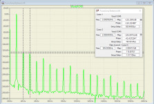
I'm also attaching the schematic in its present state, the testbench schematic, and FFTs of the latest amp at 1 kHz and 1W, 10W, and 100W. Finally, I have attached the amp netlist and .asc file.
I think the low frequency circuit design is finished. I had hoped to get high frequency THD lower, but the low frequency distortion is a lot lower than I expected. Two-pole compensation may help me, now that the output stage distortion is a lot lower. For the record, I do not expect to realize 20u% THD or even 100u% THD. Like Camelot, it's only a model.
Then I'll decide if I want a DC servo to kill offset. Then I need to decide how I'll do speaker protection, and how I'll generate the 70V rails. I already have the transformer, rectifiers, and rail caps chosen.
Ten days ago, I said I was going to optimize the output stage. Then I got busy at work, and had to put this aside for a bit.
The optimization has gone better than I expected. To review the evolution of the performance so far, I'm attaching the THD vs freq & power plots of
- The original circuit with KSC2690/A1220 drivers.
- The revised circuit with 4 each of KSC3503/A1381 as drivers.
- The revised circuit with pre-driiver and driver currents optimized. Output is also boosted a bit, from 70mA per let to 100mA.
I'm also attaching the schematic in its present state, the testbench schematic, and FFTs of the latest amp at 1 kHz and 1W, 10W, and 100W. Finally, I have attached the amp netlist and .asc file.
I think the low frequency circuit design is finished. I had hoped to get high frequency THD lower, but the low frequency distortion is a lot lower than I expected. Two-pole compensation may help me, now that the output stage distortion is a lot lower. For the record, I do not expect to realize 20u% THD or even 100u% THD. Like Camelot, it's only a model.
Then I'll decide if I want a DC servo to kill offset. Then I need to decide how I'll do speaker protection, and how I'll generate the 70V rails. I already have the transformer, rectifiers, and rail caps chosen.
Attachments
-
 THD_1kHz_100W_FFT_28Mar2021.PNG54.2 KB · Views: 173
 -
 THD_1kHz_10W_FFT_28Mar2021.PNG56.1 KB · Views: 179
 -
 THD_1kHz_1W_FFT_28Mar2021.PNG53.5 KB · Views: 227
 -
 Testbench_29Mar2021.PNG54.4 KB · Views: 456
 -
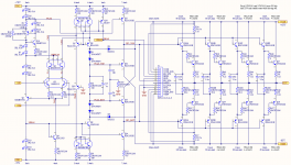 AutoBias200_29Mar2021.PNG214.9 KB · Views: 482
 -
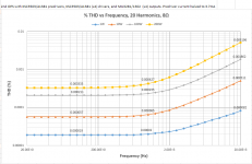 THDvsF_v2_optimized.PNG47.9 KB · Views: 461
 -
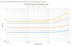 THDvsF_v2.PNG34.8 KB · Views: 423
 -
 THDvsF_v1.PNG40.8 KB · Views: 424
 -
Power_Amp_200W.txt14.5 KB · Views: 100
-
PowerAmpTestbench.asc4.6 KB · Views: 139
Looking really good.
I'll most likely build a pair of mono blocks. Undecided what to build I have had two 550VA 2x50VAC toroidals, capacitors, and two beefy heatsinks sitting around for quite some time now🙂
I'll most likely build a pair of mono blocks. Undecided what to build I have had two 550VA 2x50VAC toroidals, capacitors, and two beefy heatsinks sitting around for quite some time now🙂
In addition to the output stage changes, R5 now has the same value as R7 🙂.
I had been wondering what your thinking is regarding current mirror design and balancing of base currents.
BTW, may I bring your attention to the Stax DA-100M? I think that you may enjoy looking at the schematic.
http://www.amplimos.it/images/engine_stax_da-100m_schematic.pdf
kind regards, jonathan
I had been wondering what your thinking is regarding current mirror design and balancing of base currents.
BTW, may I bring your attention to the Stax DA-100M? I think that you may enjoy looking at the schematic.
http://www.amplimos.it/images/engine_stax_da-100m_schematic.pdf
kind regards, jonathan
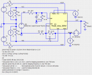
SLABS layout update
The SLABS layout update is done. With the two TO-220 passing transistors and their heatsink we are still on the 2"x2" PCB formfactor.
The heatsink is the inexpensive ATS-PCB1072, available at Mouser and nearly all venders. The transistors and heatsinks are bolted back to back with a couple of flat washers or a spacer in between the heatsinks to keep an air gap. I think that will be a very sturdy installation.
Below is the 3-D rendering. The through bolt, insulator, thermal interface material, and the spacer are not shown. The KiCAD schematic/layout files will follow soon.

Russell, I'm not sure this concern I have is valid or not, that the simulation suggests the TL084 would draw 5mA each opamp, totaling 20mA for the package. That makes a dissipation of 600mW at +/-15V, 88% of its 680mW limiting (up to 60C amb). I didn't realize it until you pointed out those passing transistors in the rail regulators have to be TO-220 and be heat-sunk.
The simulation seems to work fine with +/-12V, though I did tweak the resistor divider to maintain the same Vref. Would you think lowering the supply by a few volts is a good idea?
The SLABS layout update is done. With the two TO-220 passing transistors and their heatsink we are still on the 2"x2" PCB formfactor.
The heatsink is the inexpensive ATS-PCB1072, available at Mouser and nearly all venders. The transistors and heatsinks are bolted back to back with a couple of flat washers or a spacer in between the heatsinks to keep an air gap. I think that will be a very sturdy installation.
Below is the 3-D rendering. The through bolt, insulator, thermal interface material, and the spacer are not shown. The KiCAD schematic/layout files will follow soon.
Russell, I'm not sure this concern I have is valid or not, that the simulation suggests the TL084 would draw 5mA each opamp, totaling 20mA for the package. That makes a dissipation of 600mW at +/-15V, 88% of its 680mW limiting (up to 60C amb). I didn't realize it until you pointed out those passing transistors in the rail regulators have to be TO-220 and be heat-sunk.
The simulation seems to work fine with +/-12V, though I did tweak the resistor divider to maintain the same Vref. Would you think lowering the supply by a few volts is a good idea?
In addition to the output stage changes, R5 now has the same value as R7 🙂.
I had been wondering what your thinking is regarding current mirror design and balancing of base currents.
BTW, may I bring your attention to the Stax DA-100M? I think that you may enjoy looking at the schematic.
http://www.amplimos.it/images/engine_stax_da-100m_schematic.pdf
kind regards, jonathan
Hi, Jonathon,
I had tweaked R7 to zero out the DC offset of the amplifier, for open loop studies of DC transfer function. I never intended for the final amp to have different values for R5 and R7. OTOH, I may yet set them to different values, and inject a current into the emitter of Q30 to zero the amp's DC offset.
It doesn't hurt anything besides offset for those two currents to be slightly mismatched. In this case, I was correcting input offset, making the input pair run exactly the same current.
Ha ha, that STAX amplifier looks familiar in many respects. I swear I have never seen that schematic before. Its CF output stage is a little complicated for my taste, but it would let me linearize the OPS without relying on high frequency global loop gain. I'm really trying to keep this amp to a single gain stage.
That looks really good. I'll be happy to see the files.The SLABS layout update is done. With the two TO-220 passing transistors and their heatsink we are still on the 2"x2" PCB formfactor.
The heatsink is the inexpensive ATS-PCB1072, available at Mouser and nearly all venders. The transistors and heatsinks are bolted back to back with a couple of flat washers or a spacer in between the heatsinks to keep an air gap. I think that will be a very sturdy installation.
Below is the 3-D rendering. The through bolt, insulator, thermal interface material, and the spacer are not shown. The KiCAD schematic/layout files will follow soon.
View attachment 936714
Russell, I'm not sure this concern I have is valid or not, that the simulation suggests the TL084 would draw 5mA each opamp, totaling 20mA for the package. That makes a dissipation of 600mW at +/-15V, 88% of its 680mW limiting (up to 60C amb). I didn't realize it until you pointed out those passing transistors in the rail regulators have to be TO-220 and be heat-sunk.
The simulation seems to work fine with +/-12V, though I did tweak the resistor divider to maintain the same Vref. Would you think lowering the supply by a few volts is a good idea?
I'm not using the standard TL084 here, but the TL084H. Each op amp draws about 1 mA. Datasheet from TI says a regular TL084 draws 1.4mA/op amp, 2.8mA max. So, power dissipation should be around 1/3 of what your simulation shows. SPICE models for op amps often get supply current wrong. Many of them don't draw current from the supplies at all. The vast majority of TL084 are powered from +/-15V, so I do not expect problems.
Regarding the lower supply. The lower supply slightly limits how fast the op amp can pull the minimum hold cap down, but it should be negligible. +/-12V is fine, but should not be necessary.
Now you're probably thinking that I told you wrong about needing to heat sink the pass transistors. Sorry. I like to be conservative with those.
- Home
- Amplifiers
- Solid State
- RK-Auto200W Amplifer