UMS = Universal Mounting Specifications, I thought. See DIYAudio Shop.
Best regards!
https://diyaudiostore.com/pages/universal-mounting-specification
To save the hunt. 🙂
Good work, as always Valery, nice to see you are making it 100x100mm
Just some thoughts here, it is your design, so obviously it is your choice 🙂
This is one that I think that I will build. If Jeff builds it I can share some pcbs with him as I would order from pcbway since they are so economical.
Just wondering if you or anyone else, Terry Y. comes to mind, will continue to build their own pcbs anymore knowing that we can get 10 pro pcbs from pcbway for $5?
If you make it 2 sided, could you generate the top copper layer/solder mask/silkscreen which would take place of the 1 sided pcb connection jumpers and add a copper area fill for a ground plane?
The other thing that I see is the nfb connections require a wire link, to the ops. I assume the other ops conns are the same wire links. Is it possible to put the "nfb" on the pcb edge lined up with the other connectors so that one could use right angle connectors to mate with the ops pcb? It is nice to be able to eliminate wiring as much as possible? What are those connectors for the ops, AMP/TE MTA156? type or something else?
Will you supply gerber/drill data or just pdf data? I assume you are working in multi-sim?
And for the ops, what are the options available? I have some alfets ALF16N(P)16 left from my OPC wire amp LME49830 build that I could use. I would also like to try a non-switching ops also. I have a couple of used Pioneer SX-1250 transformers(~600VA) that I would like to use. I could layout a ops fairly easily in the 100x100mm form factor and offer it for others to use.
Cheers
Rick
Last edited:
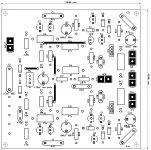
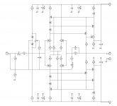
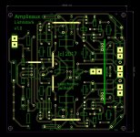
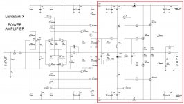
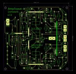
Lichtstark TH v1.0 - full package
Hello All,
Here is the full package, including both gerbers and pdf files for etching, as well as the hi-res schematic in pdf.
Right now it's set for +/-70V rails. For lower rails a few resistor values must be amended - let me know the desired voltage, I will come back to you with the values.
Have fun! Note - this is v1.0, so the need for some fine-tuning may arise before it becomes a mature "product". As soon as you build it - first test it standalone. Let me know is you will have questions.
Cheers,
Valery
Attachments
Good work, as always Valery, nice to see you are making it 100x100mm
Just some thoughts here, it is your design, so obviously it is your choice 🙂
This is one that I think that I will build. If Jeff builds it I can share some pcbs with him as I would order from pcbway since they are so economical.
Just wondering if you or anyone else, Terry Y. comes to mind, will continue to build their own pcbs anymore knowing that we can get 10 pro pcbs from pcbway for $5?
If you make it 2 sided, could you generate the top copper layer/solder mask/silkscreen which would take place of the 1 sided pcb connection jumpers and add a copper area fill for a ground plane?
The other thing that I see is the nfb connections require a wire link, to the ops. I assume the other ops conns are the same wire links. Is it possible to put the "nfb" on the pcb edge lined up with the other connectors so that one could use right angle connectors to mate with the ops pcb? It is nice to be able to eliminate wiring as much as possible? What are those connectors for the ops, AMP/TE MTA156? type or something else?
Will you supply gerber/drill data or just pdf data? I assume you are working in multi-sim?
And for the ops, what are the options available? I have some alfets ALF16N(P)16 left from my OPC wire amp LME49830 build that I could use. I would also like to try a non-switching ops also. I have a couple of used Pioneer SX-1250 transformers(~600VA) that I would like to use. I could layout a ops fairly easily in the 100x100mm form factor and offer it for others to use.
Cheers
Rick
Thank you Rick 😀
With regards to OPS - attached combination looks very good (that's the one we use in our VHex+ amplifiers). It's simple and great performing. If you can lay it out (everything that's within the red frame) - it would be cool.
In fact, Didiet has already done it in the other thread, but with 2 pairs of output devices it's bigger than 100mm x 100mm:
http://www.diyaudio.com/forums/solid-state/294632-sons-vhex-42.html#post4960173
Also, combinations with the Slewmaster OPS modules can be tested - it should be fully compatible with them.
NFB connection - not enough space on the edge of the board, also - on many OPS boards it's not on the edge as well (it may be even placed close to the opposite edge, near the output), so a separate wire for NFB is not a problem normally.
Front-end module for NS Modular OPS carrier board will be available from us soon - I start working on it.
Cheers,
Valery
Attachments
Hi Valery,
I took a look at your fab data, I noticed a few things.
1) I see that the holes for the wire jumpers on the top (trace on top copper layer) have no solder mask openings(flash apertures) for the plated thru holes on either top or bottom s/mask layers. It will be very hard to solder to those pad on either side, since they will be flooded with soldermask, that will slurp into the holes. It is fine if you do not use s/mask 🙂
2) Bottom Paste layer? It should be named a bottom silk layer.
That is all I see now 🙂
Cheers
Rick
Rick, you're right - I normally have my vias covered by mask in Diptrace settings for double-sided boards. I will open the holes in the mask tomorrow.
Bottom paste sounds funny - I will check it as well 🙂
Bottom paste sounds funny - I will check it as well 🙂
Hi Jeff,
A bit of pcb assembly process trivia for you.
When I worked for HP, in the 90's, they had a pcb assembly process called "paste in hole", SMT2PTH, where they pasted through hole component pads (using a stencil) for a reflow process. This was for mixed tech assemblies, SMT and THT combined to eliminate an extra wave solder process step. It was quiet involved, they wrote custom software, for the Mentor BS eCAD toolset, to automatically build the component pad stack. It involved a formula based the hole size, lead diameter, pcb thickness, stencil thickness.
Rick
I'm out of town right now. When I get back, if no one has built this I will etch a couple of boards and test it.
Blessings, Terry
Blessings, Terry
New Gerber's looks good Valery. I think it is good to fab from now. The pcb fab mfg may flag #5 below at data inspection. See some of the assembly issues below.
I know I might be a bit over critical, this is DIY after all, but I once did these design reviews for a living 🙂 Take it or leave it, it is your choice.
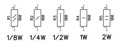
1) When looking at the schematic, I see two different resistors symbols, one with a horizontal line( i.e. R4) and some with a forward slant(i.e. R8), in the symbol body. Is there any significance to the difference?
There is no title block in the schematic, it helps identify information, such as design name, revisions,dates, authors etc. Someone to point a finger at
2) BOM? The only part that is not obvious is the connectors, but some resistors may be more than the std 1/4W,1% MF types. Usually one puts a note saying something like 1/4W,1% unless otherwise noted.
3) I measure some of the film cap lead spacings and they are not std spacing like 5,7.5,10,15mm. Like C7, its pin-pin spacing is 11.43mm? Yes I know it is all in the libraries, just that 11.43mm spacing limits your component choices. Do you really want to have to do odd size lead forming. Most film caps have std lead spacing for automatic assembly in mind.
C11=5.08mm
C1=14.7mm
C2=11.43mm
You must be using the eCAD supplied libraries, I assume 😱 we all know they are problematic, they do not know much about DFM, it has always been a problem with all the eCAD tool mfgs. Some are still stuck in the mil->mm conversion era, stucking with std 100 mil spacings, i.e. C11=5.08mm (200mil)
4) I see a duplicate entry in the drill schedule and the drill tools, round 1.17mm(46mil). Not a big or show stopper issue, I know when I use ORCAD 16, it does the same, if I have any difference in a pad stack construction. The pcb fab mfg can deal with it, they just see two identical tools (T5,T6) in the drill data.
5) This one is strange 😕 , the 4 mounting holes are not shown in the "plated_through" layer or in the drill schedule but they are in the drill data, identified as using tool T10(3.17mm)
There is also no top/bottom soldermask around the holes which could be flagged as a violation. Usually one would make a mounting tooling hole un-plated since there is no connectivity and un-plated holes have higher tolerances. But for pcb fabs like pcbway they only offer plated holes (for the cheap process), so you are correct in making it plated. Some times they flag a plated through hole that has no annular ring, but pcbway has not done this for me.
6) Since I see Jeff's name on the pcb, what was his task in this design? Is Jeff your pcb design service arm of the development team or does he play another function?
Glad to be of service 😱 like it or not
Cheers
Rick
I know I might be a bit over critical, this is DIY after all, but I once did these design reviews for a living 🙂 Take it or leave it, it is your choice.
1) When looking at the schematic, I see two different resistors symbols, one with a horizontal line( i.e. R4) and some with a forward slant(i.e. R8), in the symbol body. Is there any significance to the difference?
There is no title block in the schematic, it helps identify information, such as design name, revisions,dates, authors etc. Someone to point a finger at
2) BOM? The only part that is not obvious is the connectors, but some resistors may be more than the std 1/4W,1% MF types. Usually one puts a note saying something like 1/4W,1% unless otherwise noted.
3) I measure some of the film cap lead spacings and they are not std spacing like 5,7.5,10,15mm. Like C7, its pin-pin spacing is 11.43mm? Yes I know it is all in the libraries, just that 11.43mm spacing limits your component choices. Do you really want to have to do odd size lead forming. Most film caps have std lead spacing for automatic assembly in mind.
C11=5.08mm
C1=14.7mm
C2=11.43mm
You must be using the eCAD supplied libraries, I assume 😱 we all know they are problematic, they do not know much about DFM, it has always been a problem with all the eCAD tool mfgs. Some are still stuck in the mil->mm conversion era, stucking with std 100 mil spacings, i.e. C11=5.08mm (200mil)
4) I see a duplicate entry in the drill schedule and the drill tools, round 1.17mm(46mil). Not a big or show stopper issue, I know when I use ORCAD 16, it does the same, if I have any difference in a pad stack construction. The pcb fab mfg can deal with it, they just see two identical tools (T5,T6) in the drill data.
5) This one is strange 😕 , the 4 mounting holes are not shown in the "plated_through" layer or in the drill schedule but they are in the drill data, identified as using tool T10(3.17mm)
There is also no top/bottom soldermask around the holes which could be flagged as a violation. Usually one would make a mounting tooling hole un-plated since there is no connectivity and un-plated holes have higher tolerances. But for pcb fabs like pcbway they only offer plated holes (for the cheap process), so you are correct in making it plated. Some times they flag a plated through hole that has no annular ring, but pcbway has not done this for me.
6) Since I see Jeff's name on the pcb, what was his task in this design? Is Jeff your pcb design service arm of the development team or does he play another function?
Glad to be of service 😱 like it or not
Cheers
Rick
Last edited:
I'm out of town right now. When I get back, if no one has built this I will etch a couple of boards and test it.
Blessings, Terry
Hi Terry - very cool, I was actually expecting you to jump in!
It would be nice to test it standalone and then to try some OPS options - you've got enough of them for sure.
Cheers,
Valery
Hi Rick!
Yes, you take it a bit more serious than I normally do 😀
On the other hand, I'm always happy to take a good advise and improve my designs in the future.
This is the way resistor's power ratings are marked in Russia during long time - rather convenient, in my opinion. See the picture attached.
BOM - possible, I do it sometimes, although it requires some hand-editing after it's generated by Diptrace.
I've got different libraries - just used this one some time ago and then copying/pasting some parts. OK - point taken, I will try to use more standard spacings.
That's because of the "easy" way I solved the mask issue - simply added a test point on top of each via - that's why those are two elements and two holes at the same place.
I have never looked into it - the holes I get from PCB house are fine - so... just didn't see any issue.
We are a team - Jeff does a lot of control board circuit design work, all sort of layout work (most of NS Modular layouts are done by him), microcontroller code updates, great metal works, prototyping, testing, etc. We often put both names on what we do, regardless of the real level of involvement in each particular case. This one is done by me, but we are the team anyway
As I mentioned - thank you for the comments, I take a note and improve with every new design
Cheers,
Valery
New Gerber's looks good Valery. I think it is good to fab from now. The pcb fab mfg may flag #5 below at data inspection. See some of the assembly issues below.
I know I might be a bit over critical, this is DIY after all, but I once did these design reviews for a living 🙂 Take it or leave it, it is your choice.
Yes, you take it a bit more serious than I normally do 😀
On the other hand, I'm always happy to take a good advise and improve my designs in the future.
1) When looking at the schematic, I see two different resistors symbols, one with a horizontal line( i.e. R4) and some with a forward slant(i.e. R8), in the symbol body. Is there any significance to the difference?
There is no title block in the schematic, it helps identify information, such as design name, revisions,dates, authors etc. Someone to point a finger at
This is the way resistor's power ratings are marked in Russia during long time - rather convenient, in my opinion. See the picture attached.
2) BOM? The only part that is not obvious is the connectors, but some resistors may be more than the std 1/4W,1% MF types. Usually one puts a note saying something like 1/4W,1% unless otherwise noted.
BOM - possible, I do it sometimes, although it requires some hand-editing after it's generated by Diptrace.
3) I measure some of the film cap lead spacings and they are not std spacing like 5,7.5,10,15mm. Like C7, its pin-pin spacing is 11.43mm? Yes I know it is all in the libraries, just that 11.43mm spacing limits your component choices. Do you really want to have to do odd size lead forming. Most film caps have std lead spacing for automatic assembly in mind.
C11=5.08mm
C1=14.7mm
C2=11.43mm
You must be using the eCAD supplied libraries, I assume 😱 we all know they are problematic, they do not know much about DFM, it has always been a problem with all the eCAD tool mfgs. Some are still stuck in the mil->mm conversion era, stucking with std 100 mil spacings, i.e. C11=5.08mm (200mil)
I've got different libraries - just used this one some time ago and then copying/pasting some parts. OK - point taken, I will try to use more standard spacings.
4) I see a duplicate entry in the drill schedule and the drill tools, round 1.17mm(46mil). Not a big or show stopper issue, I know when I use ORCAD 16, it does the same, if I have any difference in a pad stack construction. The pcb fab mfg can deal with it, they just see two identical tools (T5,T6) in the drill data.
That's because of the "easy" way I solved the mask issue - simply added a test point on top of each via - that's why those are two elements and two holes at the same place.
5) This one is strange 😕 , the 4 mounting holes are not shown in the "plated_through" layer or in the drill schedule but they are in the drill data, identified as using tool T10(3.17mm)
There is also no top/bottom soldermask around the holes which could be flagged as a violation. Usually one would make a mounting tooling hole un-plated since there is no connectivity and un-plated holes have higher tolerances. But for pcb fabs like pcbway they only offer plated holes (for the cheap process), so you are correct in making it plated. Some times they flag a plated through hole that has no annular ring, but pcbway has not done this for me.
I have never looked into it - the holes I get from PCB house are fine - so... just didn't see any issue.
6) Since I see Jeff's name on the pcb, what was his task in this design? Is Jeff your pcb design service arm of the development team or does he play another function?
We are a team - Jeff does a lot of control board circuit design work, all sort of layout work (most of NS Modular layouts are done by him), microcontroller code updates, great metal works, prototyping, testing, etc. We often put both names on what we do, regardless of the real level of involvement in each particular case. This one is done by me, but we are the team anyway
Glad to be of service 😱 like it or not
As I mentioned - thank you for the comments, I take a note and improve with every new design
Cheers
Rick
Cheers,
Valery
Hi Valery,
Yeah I thought that R symbol would have some meaning, just need to know what it means. Nothing attached that I can see 🙂 No rush, have a nice Easter weekend
Happy eater eggs
P.S. Do you do the painted boiled eggs tradition? When my Dad was alive, he was Greek Orthodox, he would dye the boiled eggs, red and we would have a contest to smash each others egg ends against each others, to determine a winner, do you do this tradition?
Rick
Are your Dad from Greece?Hi Valery,
Yeah I thought that R symbol would have some meaning, just need to know what it means. Nothing attached that I can see 🙂 No rush, have a nice Easter weekend
Happy eater eggs
P.S. Do you do the painted boiled eggs tradition? When my Dad was alive, he was Greek Orthodox, he would dye the boiled eggs, red and we would have a contest to smash each others egg ends against each others, to determine a winner, do you do this tradition?
Rick
My Grandparents on my Fathers side came from Greece, in the early 1900's. Grandpa was a confectioner. Dad said they were Spartan's from Peloponnese peninsula. Story was the Savas (Sabbas, no "V" in the greek dictionary) clan were rebel's living in the mountains that the Turk's never got to during their invasion & rule. Turk's supposedly destroyed all the records. One day, I would like to visit the place where they came from. To many generations now, family lost touch with relatives back home. Maybe you know some of those rebels? 🙂
Hi Valery,
Yeah I thought that R symbol would have some meaning, just need to know what it means. Nothing attached that I can see 🙂 No rush, have a nice Easter weekend
Happy eater eggs
P.S. Do you do the painted boiled eggs tradition? When my Dad was alive, he was Greek Orthodox, he would dye the boiled eggs, red and we would have a contest to smash each others egg ends against each others, to determine a winner, do you do this tradition?
Rick
I forgot to attach this picture to the previous message 😛
Yes, there is such a tradition - people paint those boiled eggs - sometimes some solid color, sometimes - some creative ornament, and then have a contest to smash each others egg ends against each others, to determine a winner 😀
Attachments
Therefore you have Greek blood in your veins!My Grandparents on my Fathers side came from Greece, in the early 1900's. Grandpa was a confectioner. Dad said they were Spartan's from Peloponnese peninsula. Story was the Savas (Sabbas, no "V" in the greek dictionary) clan were rebel's living in the mountains that the Turk's never got to during their invasion & rule. Turk's supposedly destroyed all the records. One day, I would like to visit the place where they came from. To many generations now, family lost touch with relatives back home. Maybe you know some of those rebels? 🙂
Moreover, our ancestors were neighbors. The distances between Agrinion Peloponnesos is very small.
Yes i know some of those rebels but from 2nd World War.

Ιf in the future you will visit the GREECE I will be glad to meet you!
Valery,sorry for this of topic.🙂
Happy Easter.
Last edited:
- Home
- Amplifiers
- Solid State
- Revisiting some "old" ideas from 1970's - IPS, OPS