
Lol thank you, I’ll correct that next time - the wonkyness of the diodes is already starting to annoy me.
Hmm notification OPA1678 planned ship 03 Nov 2023.. so i may look around for alternative suppliers.
A little more added - some of my resistors on this board are also backordered along with the OPA.
I use my own method for soldering the chips to the pads - I use a small dollop of paste on each corner pin, position the chip and then put the iron next to the dollop allowing the heat todo the work to soldier the corner pin without moving the chip. I then do the same with the other corner. Next I put a very thin line of paste alongside the pins then use the flat edge of the iron to drag along side on the solder pad - leaving the capillary action to draw the solder between the pad and chip pin. After I have done both sides I re-apply heat to the leg to ensure the solder joint is both the pad and the pin.

I corrected D4, and the SOT23s I found easier with the larger iron head (after this photo I neaten up with the large tip on. I'm only using an unregulated 25W antex iron, so it can be done you just have to understand that big pads/pours will suck the heat away quickly. Just be careful of a hot iron a going into the centre of the paste, the flux then sprays the molten paste, instead it's better to edge up to the solder and let the heat warm through it.
I'm leaving the big components so I can flip the board over and it will stay flat.
I use my own method for soldering the chips to the pads - I use a small dollop of paste on each corner pin, position the chip and then put the iron next to the dollop allowing the heat todo the work to soldier the corner pin without moving the chip. I then do the same with the other corner. Next I put a very thin line of paste alongside the pins then use the flat edge of the iron to drag along side on the solder pad - leaving the capillary action to draw the solder between the pad and chip pin. After I have done both sides I re-apply heat to the leg to ensure the solder joint is both the pad and the pin.
I corrected D4, and the SOT23s I found easier with the larger iron head (after this photo I neaten up with the large tip on. I'm only using an unregulated 25W antex iron, so it can be done you just have to understand that big pads/pours will suck the heat away quickly. Just be careful of a hot iron a going into the centre of the paste, the flux then sprays the molten paste, instead it's better to edge up to the solder and let the heat warm through it.
I'm leaving the big components so I can flip the board over and it will stay flat.
I used NE5532AD as I found the same issue as you, I have OPA1678 on order but it will be Nov.Hmm notification OPA1678 planned ship 03 Nov 2023.. so i may look around for alternative suppliers.
Hi, everybody!
Thanks @MarcelvdG for sharing this beatiful project and the other projects you have made. I have been learning a lot from the projects your shared during the last many years.
I just finished the lite_for_RPi vesion of this RTZ FIRDAC and even if it is a downgraded variant (no ref. voltage circuit, but only an LT3045 based power supply) it still sounds amazing.
Attachments

I'm not familiar with that DAC. Are you mixing me up with someone else or is this a variant you designed?
Yes, it is a modified variant.
@ digital side - I replaced the voltage ref. you designed with a simple power supply, due to the space limitations, so this is the biggest downgrade.
I also replaced 1x 74AHCT74 (U20A+U20B) with 2 x 74LVC1G74, and used an FPGA (as I2S master for RPi, 256x interpolation and SD modulator) on the same PCB..
@ analog side - I didn't had 2 x OPA210 so I replaced them with 1 x OPA2210, replaced OPA1678 with MUSES8820, added a diferential to single output stage and used different mute relays and circut.
Inspired from your Valve Project, I use 2 modes: "PWM8" (multibit dithered quantizer) and "CHAOS" (single bit undithered).
Which of the modes do you prefer?
It looks like you have an FPGA in a ball grid array package. What method did you use to solder it?
It looks like you have an FPGA in a ball grid array package. What method did you use to solder it?
Not sure about the prefered mode yet, I need more listening time. 🙂
I have the cheapest reflow oven in the market, T-962, which is good enough for a hobbiest. Had no stencil, so fpga was soldered first in the oven and the other parts later by hand, using soldering station and heat gun. I spent about 2 hours to solder 0402 size caps, 18 pcs. only, on the bottom side, below fpga.🤓
I have the cheapest reflow oven in the market, T-962, which is good enough for a hobbiest. Had no stencil, so fpga was soldered first in the oven and the other parts later by hand, using soldering station and heat gun. I spent about 2 hours to solder 0402 size caps, 18 pcs. only, on the bottom side, below fpga.🤓
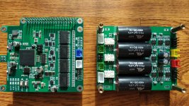
Finished the DAC board except thr connectors and four backordered resistors. About 50% through the filter board.
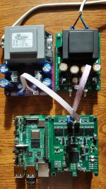
Next task is testing everything to ensure no shorts and order some additional connectors (ordered 1 not 3), plus some other bits for another project.
Probably one of the hardest/logest soldering builds with the soldering iron I’ve done. Spent over an hour looking for one of the 8 smaller caps that dissappeared.. eventually found on the carpet.
You'll probably find you've soldered in a bit of sock fluff. Not sure of the capacitance of that!? 🤓
@MarcelvdG, just stumbled across this project. Impressive! Both the engineering and the build. Nice that it comes together so well! Very educational and inspiring. I've a hard time figuring out what it all does but think I get the global picture how it sort of works 😊 . Still, as I'm a bit of a noob: as I understand it correctly, the DSD signal is already split into left and right before it enters the DAC? And is that always the case with DSD?
Raw (also known as native) DSD interfaces normally have separate data lines for left and right, and that is the only format that my RTZ shift register DAC supports.
There are other ways to transport DSD signals where left and right are time multiplexed onto the same data line, for example DoP (which stands for DSD over PCM, which is a trick to transport DSD signals over interfaces that were originally meant for PCM). This DAC doesn't support DoP.
My build looks like this: https://www.diyaudio.com/community/threads/return-to-zero-shift-register-firdac.379406/post-6978301 I think everyone else's builds look better, especially Thorp's variant. Anyway, it works.
Last edited:
- Home
- Source & Line
- Digital Line Level
- Return-to-zero shift register FIRDAC