Yes, see post #2266, https://www.diyaudio.com/community/threads/return-to-zero-shift-register-firdac.379406/post-7621479 In this example, the sum of the positive outputs is constant and the sum of the negative outputs is constant - except for glitches due to unequal rise and fall times, of course.
Marcel, but that concept does not reflect the hardware of your DAC. You have the hardware in place to allow for it to work like that.
But you are running two DAC's directly in parallel without shifting the data, clock etc. in such a way that the outputs from the two DAC's in place are "interleaved". Instead all that happens is that everything exists twice in parallel, with some heuristic attempt to compensate "on chip" and PCB variations between the two IC.
Then the clock rate must such be that the zero "holes" are filled by timing alternation as data ripples through the shift register, in which case the I/V opamps don't see zeros. Is that correct?
The clock rate does not come into it.
A RTZ DAC must have the "holes", it's fundamental.
However you can use two (or more) actual DAC's with correct time shifted Data / Clock / Both to "fill in the hole".
It kinda became clear to me because I have been a lot of work in recent times on power supplies for industrial application SMPS that ended up using multiple switching IC's interleaved from where the logical progression led into DC to AC converters (aka class D Amplifier) using multiple interleaved IC's with BD modulation to allow very different approaches to filtering and from there into DAC's.
In each case Interleaving ultimately pull a Phil A Void (the imaginary inventor of the Void Turntable) and fill in "holes" removing or mitigating against noise that is quite troublesome.
Thor
Yes, but holes are there before the resistors. After the resistors there is a summing bus. All we need to do to see what is really happening is remove the output stage board and take a look with a scope, maybe with a low value load resistor on the summing bus. Either the holes will be there before the resistors or not, and holes will be on the summing bus or not.RTZ DAC must have the "holes", it's fundamental.
Isn’t it the right time now to simulate Marcel’s Firdac versus the various proposals going around to clearly show the differences and possible benefits of whatever nature.
I did that with Marcels Solid State Firdac using randomized rise and fall times for all digital components to create glitches and DC errors.
In the end, with the help of these sims, Marcel could convince me of that his design could remove all doubts.
Hans
I did that with Marcels Solid State Firdac using randomized rise and fall times for all digital components to create glitches and DC errors.
In the end, with the help of these sims, Marcel could convince me of that his design could remove all doubts.
Hans
Yes, but holes are there before the resistors.
Let us rephrase that.
In front of the resistors we have a waveform with nanosecond risetime that switches between 0V and 5V. This causes current flow in the resistor. In other words, the complete DAC creates current pulses that are send into a "virtual earth".
Part of that is also that a (say) NRZ waveform is altered in an RTZ DAC to have significant added common mode component not present with NRZ.
After the resistors there is a summing bus. All we need to do to see what is really happening is remove the output stage board and take a look with a scope
You can look with the 'scope with the output stage attached.
Either the holes will be there before the resistors or not
It's an RTZ DAC - of course they are there.
holes will be on the summing bus or not.
They will be there as current changes.
What we see elsewhere depends entirely what hang off the "bus" and how it reacts to these current changes.
I find the solution in the analogue stage for the BB DSD1700 (which was kind of the same in an IC) telling as to what the RTZ system does to the analogue stage.
First again the DSD1700 principle design:
It is a single channel DAC with individual FIR DAC's as so:
Resistors are NOT equal weight.
And here the recommended output stage:
Notice the 1k in series after the first filter stage. The whole structure causes less than ideal SNR and other issues.
Anyway, I'll leave it at this until I get around to setting up the sim.
Thor
My focus is on the I/V conversion.
Can it be concluded that the RMS values of both forms of conversion of the digital waveforms is equal, notwithstanding that transient glitches exist and notwithstanding gain differences? In other words if the analog conversion was perfect, regardless of glitches, would the two be only as distorted as the theoretical nature of the digital allows?
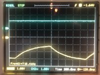
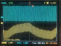
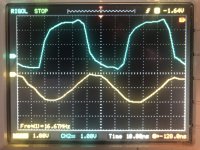
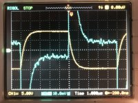
The reason for asking is that I am working on an I/V for D/A that seems could also handle such extreme signals directly, with preliminary results depicted by the screenshots below. Don't know how they compare with other networks.
1. The first screenshot depicts a 500KHz square wave feeding into a low pass filter with ~250KHz low pass response.
2.The second depicts the same square wave but with an additional 16.9344MHz signal imposed on the inverting terminal (using a clock module that was lying around intended for implementation in a Sony CD player). In this screenshot the output doesn't indicate any form of rectification or non-symmetric amplitude variation in the mix. In other words the original waveform would remain in tact if the ~17 MHz was subsequently filtered out.
3. This is an expanded scale of screenshot 2 at 10nSec/ div., showing perhaps 5nSec rise-times of the oscillator. The output shows good symmetry in rising and falling edges despite the rapid input rise/fall times. Although such signals would not be imposed at this point it demonstrates exceptional suppression of lesser amplitude signals that could become imposed there.
4. The fourth is just the output of a 100KHz square wave (yellow trace) +/- 10 Volt output (+/- 5mA into 2K Ohm) with ~250KHz low pass response. The white trace is the signal across the inverting/non-inverting terminals magnified 100x. For comparison Walter Jung conducted similar x100 tests in using an AD811.
https://cfas.waltjung.org/High_Performance_Audio_Stages_Using_TransZ_Amps.pdf
Although the scale reads 10mV/ division, with 100x magnification the scale is equivalent to 100uV/ division, meaning that the output settles to <+/-100uV in 2uSec for +/-10V (+/- 5mA) input changes.


Last edited:
Of course. But where you and Marcel seem to be in disagreement is right around in the area of the shift registers, the signals that feed into the shift registers, and the resistors and summing bus. Marcel's claim is to the effect that what he has done is equivalent to two dacs offset in time. Your claim seems to be that it will take another physical dac to do what Marcel is trying to do. We shouldn't need the output stage to settle the disagreement. Its not essential to the "one dac can or can't be equivalent to two dacs offset in time" issue. Also, if it is felt that the output current waveform is a key part of the disagreement then a shunt resistor to ground (or an offset virtual ground?) makes for a simple way to observe the current waveform. IOW, even if someone doesn't have Marcel's output stage board but does have the dac board, it should still be possible to settle the dispute, right?You can look with the 'scope with the output stage attached.
Last edited:
Yes, but holes are there before the resistors. After the resistors there is a summing bus. All we need to do to see what is really happening is remove the output stage board and take a look with a scope, maybe with a low value load resistor on the summing bus. Either the holes will be there before the resistors or not, and holes will be on the summing bus or not.
Good plan, I'll try to find time to do it next week.
For clarity, I've added notes p0...p3 and n0...n3 to show what signals should occur on what 74LV574A outputs if the DAC should happen to work the way I intended it to work.
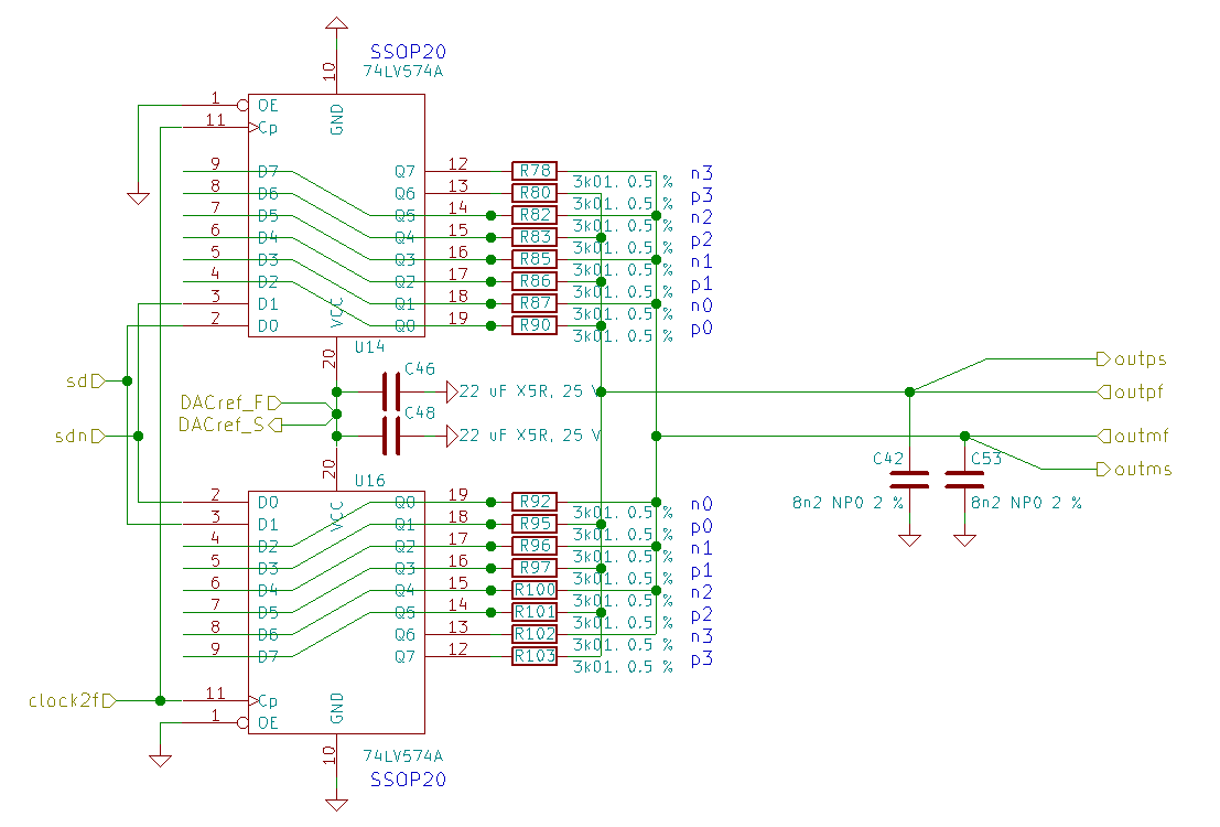
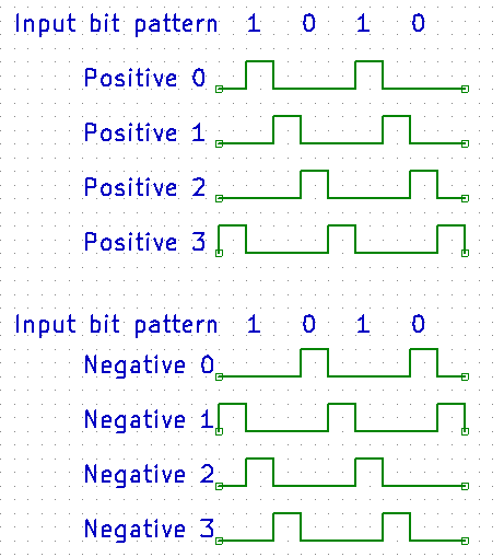
("Input bit pattern" refers to the input bit pattern of the entire DAC, not the input pattern of the 74LV574As.)
("Input bit pattern" refers to the input bit pattern of the entire DAC, not the input pattern of the 74LV574As.)
I don't see why the interleaving with shift registers would not work as Marcel described above or in post #2266. What is unclear (at least to me) is why Thor thinks this is not the case or why he thinks this interleaving is not sufficient.
But where you and Marcel seem to be in disagreement is right around in the area of the shift registers, the signals that feed into the shift registers
I am not sure it is possible to disagree with then truth tables in datasheets and a physical schematic. There is no room for opinion, in my, aeehhhmmm opinion.
and the resistors and summing bus.
No, we completely agree on that as far as his circuit is concerned.
I don't even think we in principle disagree on filtering the clock feed trough / clock harmonics / clock sub harmonics / et al passively.
It's just I prefer a 3rd order RCLC filter @ ~100kHz which gives 60dB per decade attenuation and thus 120dB attenuation at 10Mhz over a first order filter with 20dB/decade attenuation and thus only 40dB attenuation at 10MHz.
Marcel's claim is to the effect that what he has done is equivalent to two dacs offset in time.
Yes, actually MvG has done with with FOUR single BIT DAC's (giving a 4-Tap FIR filter).
But what has not done, is to interleave two DAC's in such a way that when one DAC's output is in the "Zero" phase of the RTZ cycle, the second DAC is in the "Data" phase of the RTZ cycle.
Your claim seems to be that it will take another physical dac to do what Marcel is trying to do.
I cannot answer to what MvG is trying to do. I can only share my analysis of what is actually done.
As a result I also cannot claim anything if it takes different hardware to do what MvG is trying to do.
We shouldn't need the output stage to settle the disagreement.
Agreed, Paper and IC datasheets completely suffice. That what I used in the first instance to understand the circuit.
Its not essential to the "one dac can or can't be equivalent to two dacs offset in time" issue.
There is no such issue.
There is an issue that due to the nature of RTZ DAC's large levels of common mode noise at a subharmonic of the shift register clock is created, with very substantial rise time and energy.
I suggested that one mitigation strategy for existing hardware would be to the extant second DAC and delay it's data by one shift register clock cycle, creating the "interleaving" I have been discussing and restoring all the benefits of an NRZ FIR DAC while at the same time incorporating the benefits of an RTZ DAC.
TBH I also do not see where this is in any way contentious. Extant literature covering all of this plentiful.
Also, if it is felt that the output current waveform is a key part of the disagreement then a shunt resistor to ground (or an offset virtual ground?) makes for a simple way to observe the current waveform.
The current waveform is the result of the voltage waveforms at the outputs of the shift register, which in turn are the result of the data loaded into the shift register. That data is the result of both the input data and the RTZ function.
The current waveform, with high edge rates and high common mode levels is the immediate cause of problems in the analogue stage. However it is the data send to the shift registers that is the root cause.
IOW, even if someone doesn't have Marcel's output stage board but does have the dac board, it should still be possible to settle the dispute, right?
I expect that there is no actual dispute, but rather a misunderstanding due to the relatively poorly defined meaning of "interleaved DAC's".
My use is rather specific and narrow, seemingly more so than MvG's.
I had originally kept the discussion with MvG private as I foresaw the exact happenings we see now.
People who have an emotional attachment to the original design first of all, see suggestions for improvement as criticism of both the design and designer, when it is not.
And then, instead of actually seriously looking at the issues we get defensive challenges against perceived criticism, not really trying to understand, but simply asserting that the criticism that never was criticism in the first place and it wastes everyone's time and settles nothing.
Remember, it's not important WHO is right, but WHAT is right.
Forgive me if I bow out here. I no longer have the time to use I had when younger. I have already spent more than I can justly afford. Back to stuff that pays my bills.
I said my piece. If you profit from it fine; if you don’t, too bad!
As the Marsh Arabs used say (before Saddam exterminated them): "The nature of rain is the same, but it makes thorns grow in the marshes and flowers in the gardens."
No matter what you guys do, have fun and enjoy the music.
Thor
I don't see why the interleaving with shift registers would not work as Marcel described above or in post #2266.
See here.
https://www.diyaudio.com/community/...-register-firdac.379406/page-114#post-7621717
It should be obvoius. MvG's waveform sketch show what would happen with an NRZ single Pulse. I showed what really happens in more detail.
The input to the shift register is RTZ Data. This means the data on the output of the shift register is RTZ data.
Without a mechanism to allow two DAC's to work in a way that the second DAC outputs "data" when the first outputs "zero", we get all the common mode issues inherent to RTZ (fact).
And I think the specific solution to I/U conversion and dealing with common mode is especially vulnerable to these common mode issues and causes the observed rise of HD/IMD at higher frequencies (conjecture - educated guess).
What is unclear (at least to me) is why Thor thinks this is not the case or why he thinks this interleaving is not sufficient.
Did you read my last few posts? It is spelled out as clearly as I can do.
Thor
I disagree. You seem to be missing that shift registers operate at double-speed clock. So bit shift happens at "half" of RTZ pulses resulting in similar output as with NRZ pulses at single-speed clock.MvG's waveforms show what would happen with an NRZ single Pulse.
Hi Thor,
I don't think this is an emotional issue, rather it is a technical one. But sometimes it requires taking a different tack to find some way to arrive at insight and agreement, and then move on. A simple measurement should suffice. That's all.
Personally, I would like to see you stay. You are an interesting fellow, and I know we have some mutual acquaintances.
Best,
Mark
Edit: It would also be great if you went ahead and designed a RTZ dac your way. I for one would be interested to hear it 🙂
Last edited:
I disagree. You seem to be missing that shift registers operate at double-speed clock.
Look at the linked post, I do not.
So bit shift happens at "half" of RTZ pulses resulting in similar output as with NRZ pulses at single-speed clock.
REALLY?
The SR clock clocks one bit for each half BCK cycle.
The RTZ gating inserts zero's for half each BCK cycle.
The DAC is 4 Taps long, so after two BCK cycles it will be "full".
Thus the SR contain always two "zero" separated by one BCK and two "data" separated by one BCK.
There is no mechanism that creates four times data in two BCK cycles, is there?
In order to not to have the common mode issue caused by RTZ, we would need four times "data". Simple to do with MvG's DAC - simply disable the RTZ gating, but keep running the shift register on the doubled clock. Now we are back at NRZ.
BUT in order to avoid ISI we need "zero" inserted between two "data".
In order to have both low common mode feed trough of subharmonics of the shift register clock (needs NRZ) AND no ISI (needs RTZ) we need to a mechanism that places "data" from a 50% duty cycle RTZ DAC shifted in time such that it coincides with the "zero" part from another DAC.
That is, for two BCK Cycles we now have four "zero" and four "data", causing a NRZ waveform with "glitches" at each BCK Edge which are caused by unequal rise and fall times, in common mode, but no high energy waveform ion common mode.
It really is all in great detail in my posts.
Again, I said my piece, I do not see what more to add.
Do as thou wilt, shall be the whole of the law.
Thor
Its seems simple enough. Show the waveform Marcel's dac produces as opposed to the waveform your dac would produce just before going into the output stage. It should only be necessary to show a case where an input data waveform produces different output waveforms going into the output stage (for a firdac of equal effective length and weighting). Something like that, anyway. IOW, a picture is worth a thousand words.I do not see what more to add.
Of course, on the issue of switching glitches, that may be a key difference in the waveforms.
When Marcel can produce a sequence of 16 random zero’s and ones for sdinR, and we can agree upon this pattern, I will simulate the whole Marcel circuit, and also versions with a second DAC for “interleaving” and a version with crosscoupling as in the DSD1700.
Hans
Hans
That's a good idea, Hans. This whole thing reminds me of the game show (Monty Hall) problem: https://behavioralscientist.org/ste...tch-the-monty-hall-problem-finally-explained/
"Many people can’t swallow the correct explanation even when it’s pointed out to them. This included Erdös, who, violating the soul of a mathematician, was convinced only when he saw the game repeatedly simulated."
"Many people can’t swallow the correct explanation even when it’s pointed out to them. This included Erdös, who, violating the soul of a mathematician, was convinced only when he saw the game repeatedly simulated."
Last edited:
Also, I think we need to be careful using terms like BCK. There is a BCK for the incoming DSD, but its not the same BCK that operates the shift registers. Maybe call that one BCKx2 or something. RTZ zeros are inserted on every other BCKx2 cycle. Also, the shift register is advanced on every BCKx2 cycle. So a data 1 that has had an RTZ zero inserted will repeat time shifted by BCK/2, with the intent of filling in the hole of the first. However, the zero hole will also be repeated on the next BCKx2 cycle.
The question then is how does that compare to a time offset 2nd dac that is producing data 1's with following holes? Eventually the 1's and RTZ holes will be summed somehow with the first dac. Or is the summing logic different?
The question then is how does that compare to a time offset 2nd dac that is producing data 1's with following holes? Eventually the 1's and RTZ holes will be summed somehow with the first dac. Or is the summing logic different?
It would also be great if you went ahead and designed a RTZ dac your way.
I already decided against using RTZ - on MvG's prompting a better option in our private conversation.
I for one would be interested to hear it 🙂
I think you will have the chance. It is however by far more complex than MvG's RTZ DAC.
I found it rather refreshing, however once I got my head around all the discrete logic without any diagrams of signals etc. I felt that the same hardware with minor adjustments could be improved. So I shared my ideas with MvG, who is not keen on them.
As now a potential fidelity impairment is discussed that I have reason to believe is the material result of a specific trade-off, I decided to comment on this again. And lo and behold nobody is keen.
So you expect me to convince you all and browbeat you to do it my way?
Its seems simple enough. Show the waveform Marcel's dac produces as opposed to the waveform your dac would produce just before going into the output stage.
I did.
When Marcel can produce a sequence of 16 random zero’s and ones for sdinR, and we can agree upon this pattern,
I suggest to use "DSD Silence" (0x69h) as pattern. I use TINA TI, it has good logic models and an generator that is easily set up.
I will simulate the whole Marcel circuit, and also versions with a second DAC for “interleaving” and a version with crosscoupling as in the DSD1700.
DSD1700 is more subtle, HOWEVER it does not inerleave.
If you simulate it understand the following:
1) DSD1700 uses 75% Duty Cycle RTZ, not 50% (giving 3dB more usable level)
2) DSD1700 uses two sets of shift registers in exactly the way as MvG does, to create a geometry that minimises errors in the analogue supply. It will not show up in a simulation, UNLESS you include such effects in your sim.
3) DSD1700 is likely interleaved (two duty cycle generators are shown in the principle diagram).
3) DSD1700 uses 8-Tap FIR with weights that can be approximated indirectly from the response shown, using a suitable tool.
4) DSD1700 uses separate bit switches, it does not drive the resistors from the shift registers directly.
Arguably, a kind of discrete DSD1700, with two balanced 8-tap shift registers per channel and Kaiser window weights, a 75% Duty Cycle RTZ gate derived from MvG's current RTZ DAC would be a development likely capable of improved overall performance, at greatly increased complexity.
Thor
- Home
- Source & Line
- Digital Line Level
- Return-to-zero shift register FIRDAC