I have a bit of time before my better half wakes... I'm caffeinated enough to measure, but not so much to rattle the board to pieces. so...off we go 😀
I did a bit of the full run through again just to be sure I documented all the measurements after the new relay went in.
Current state of the amp - powered up with protection LEDs lit.
Voltage across R417: 289mV
Legs of both inductors L1 and L2 to GND: <10mV
Voltage at anode leg of D403: 44V15
Voltage at cathode leg of D403 44V00
So it seems it is in protection.
Yep!? Any chance it could be thermal per above in post #57?
Thank you for looking that up. I did some additional measurements exactly as follows. All measurements taken with black probe to chassis ground and red probe to:
Pin 1 - Junction of U1 and R409, R412: (-)200mV
Pin 2 - Junction of U1 and R407, R411 and positive side of C414: 50mV
Pin 3 - Junction of U1 and R414: 596mV
Pin 4 - It joins the negative side of C414 through the trace, but I can'd find a suitable place to ensure continuity to GND on the top side of the board. If this is vital, I'll keep digging.
Pin 5 - Junction of U1 and R419: 0V75
Pin 6 - Junction of U1 and R423: 45V0
Pin 7 - Junction of U1 and R420 (-)0V75
Pin 8 - Junction of U1 and R413: 0V65
Pin 9 - Junction of U1 and R413 (opposite side of R413 to Pin 8): 3V2
So Pin 6...??
I did a bit of the full run through again just to be sure I documented all the measurements after the new relay went in.
Current state of the amp - powered up with protection LEDs lit.
Voltage across R417: 289mV
Legs of both inductors L1 and L2 to GND: <10mV
If the circuit is in protection you should have 45 volts on both sides of D403. This would indicate no current flow, telling us the protection chip is not pulling it in.
Voltage at anode leg of D403: 44V15
Voltage at cathode leg of D403 44V00
So it seems it is in protection.
Next problem... WTF is causing protection faults?
Yep!? Any chance it could be thermal per above in post #57?
This is based on the TA7317 datasheet and schematics with marked voltages.
(Data sheet, such as it is, attached below)
The TA7317 protection chip is designed so that if everything is right, after a time delay, it pulls in a relay that connects amplifier outputs to speakers. It is intended to protect speakers by preventing DC offsets and turn on thumps from reaching them.
Power is on pin 9, ground is on pin 4 and pin 5 is connected to the chip's substrate.
Signals...
Power detect at pin 1
DC detect at pins 2 and 3
Relay driver at pin 6
Rapid turn off at pin 7
Turn on delay at pin 8
In operation...
pin 1 ... < 0.75 volts ... power detect
pin 2 ... >-1 <+1 volts ... DC detect
pin 3 ... >-1 <+1 volts ... DC detect
pin 4 ... 0 volts ... ground
pin 5 ... -0.8 volts ... chip substrate
pin 6 ... ~1.5 volts when on +Vbulk when off ... relay driver
pin 7 ... < 0.6 volts ... rapid turn off
pin 8 ... >+1.7 volts ... delay turn on cap.
pin 9 ... ~+3 volts .. chip power.
If pins 1, 2, 3, 7 and 8 are not biased correctly the relay will not energize.
At turn on or after a fault is cleared, Pin 8 is initially held to ground by a capacitor that is charged through a resistor. When the charge reaches approximately 1.6 volts, pin 6 will switch on, drawing current to energize the relay.
Thank you for looking that up. I did some additional measurements exactly as follows. All measurements taken with black probe to chassis ground and red probe to:
Pin 1 - Junction of U1 and R409, R412: (-)200mV
Pin 2 - Junction of U1 and R407, R411 and positive side of C414: 50mV
Pin 3 - Junction of U1 and R414: 596mV
Pin 4 - It joins the negative side of C414 through the trace, but I can'd find a suitable place to ensure continuity to GND on the top side of the board. If this is vital, I'll keep digging.
Pin 5 - Junction of U1 and R419: 0V75
Pin 6 - Junction of U1 and R423: 45V0
Pin 7 - Junction of U1 and R420 (-)0V75
Pin 8 - Junction of U1 and R413: 0V65
Pin 9 - Junction of U1 and R413 (opposite side of R413 to Pin 8): 3V2
So Pin 6...??
Also ... after reviewing your explanation and the schematic for U1, is the voltage at pin 8, an issue? If we have <+1V7 is that why it's not turning on and why we have +VBulk at Pin 6?
I'd change C416 & C415 without thinking about it too hard. In dog years they are 100. Use a ceramic or plastic film for C416, using an electrolytic probably saved Alesis half a cent and guarenteed the amp would fail before too long.
If you don't have a .47 uf, inspect an old TV or something, they are everywhere. The modern marking is 475 (47 exponent 5 pf) . Use 50 v, marking z is 25, others probably okay
The 100 uf @ 16 can be 25 or 50 v. Before I put the case on I'd try to make it 5000 to 10000 hours service life, but any salvage part might do now.
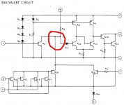
While I'll defer to an expert, the schematic clearly shows the NC contact of the relay connecting the outputs to the speaker. So it shows the relay pulling up (coil current flows) to disconnect the speakers when fault occurs.
Parade is over, watched it in glorious 13" color with 768 lines with the top of the heads cut off. 15" monitor had 30 more dried up e-capacitors, I still have 15 to install. I do have stereo hifi sound working. They actually let some bands play on screen this year!
If you don't have a .47 uf, inspect an old TV or something, they are everywhere. The modern marking is 475 (47 exponent 5 pf) . Use 50 v, marking z is 25, others probably okay
The 100 uf @ 16 can be 25 or 50 v. Before I put the case on I'd try to make it 5000 to 10000 hours service life, but any salvage part might do now.
While I'll defer to an expert, the schematic clearly shows the NC contact of the relay connecting the outputs to the speaker. So it shows the relay pulling up (coil current flows) to disconnect the speakers when fault occurs.
Parade is over, watched it in glorious 13" color with 768 lines with the top of the heads cut off. 15" monitor had 30 more dried up e-capacitors, I still have 15 to install. I do have stereo hifi sound working. They actually let some bands play on screen this year!
Last edited:
Current state of the amp - powered up with protection LEDs lit.
That's not good but it is better than yesterday.
Voltage across R417: 289mV
Legs of both inductors L1 and L2 to GND: <10mV
If you follow the schematic a bit you will discover that L1 and L2 are on the amplifier's outputs which are also fed to the TA7317 on pin 2 through R407 and R408. This forms the DC offset protection input.
Voltage at anode leg of D403: 44V15
Voltage at cathode leg of D403 44V00
So it seems it is in protection.
Now that we have continuity through the relay you can see that on the LEDS. They are fed by pin 6 of the TA7317 ... follow the schematic... Pin 6, to R423, to Q402 through J8 pin 1 to the lamp board then D310, D311, D350 and D351 to the leds.
So we have a visual test point for protection.
Yep!? Any chance it could be thermal per above in post #57?
Once again if we follow the schematic we find the termistors on the power amp pages, connected to pins 1 and 2 of J4 and J6. Following this back to the power board we discover that pin 1 is fed by the chain of R415 and R425 ... out through the thermistors, returning on pin 2 which goes to Pin 3 of the TA7317... one of the DC offset triggers.
If it was thermal pin 3 should be out of whack...
Thank you for looking that up. I did some additional measurements exactly as follows. All measurements taken with black probe to chassis ground and red probe to:
Pin 1 - Junction of U1 and R409, R412: (-)200mV
Pin 2 - Junction of U1 and R407, R411 and positive side of C414: 50mV
Pin 3 - Junction of U1 and R414: 596mV
Pin 4 - It joins the negative side of C414 through the trace, but I can'd find a suitable place to ensure continuity to GND on the top side of the board. If this is vital, I'll keep digging.
Pin 5 - Junction of U1 and R419: 0V75
Pin 6 - Junction of U1 and R423: 45V0
Pin 7 - Junction of U1 and R420 (-)0V75
Pin 8 - Junction of U1 and R413: 0V65
Pin 9 - Junction of U1 and R413 (opposite side of R413 to Pin 8): 3V2
So Pin 6...??
Pin 5 is concerning. Recheck your measurement to be sure.
If you look at the TA7317 data sheet you will see it is a substrate bias for the chip. It is connected via a diode (Q20) to the internal circuit ground (pin 4) and pulled down by R419 to the negative bulk voltage... thus it should be reading about -0.8 volts, not +0.75. This could indicate that the chip is not properly grounded (pin 4).
Also looking at the chip internal schematic we can see that Pins 2 and 3 both go through a series of switching transistors, leading to the protection triggers. Now these transistors are biased against ground (pin 4) so if the internal ground were offset from actual ground, it could falsely trigger the chip into protection... and the offset you read on pin 5 would seem to indicate that the internal ground is indeed floating.
So the next thing to try is to remove that chip --very carefully-- clean up the leads, clean up the solder pads on the board then check the land for pin 4 for continuity to ground.
If you have continuity, you likely had a bad solder point, so you can reinstall the chip and see what happens.
If you don't have continuity, you need to start following the traces and find out why.
Last edited:
I'd change C416 & C415 without thinking about it too hard.
Not every problem is about capacitors. In fact, I doubt that's the issue here at all. It appears from a quick check bypassing the relay, there are a couple of perfectly good amplifiers behind that non-energized relay.
Our friend needs to locate the actual fault and fix it first. Then we can worry about things like capacitors and the ages of parts.
While I'll defer to an expert, the schematic clearly shows the NC contact of the relay connecting the outputs to the speaker.
The schematic is drawn poorly.
The TA7317 has a delay turn on function that pulls the relay in after a time determined by R413 and C415. This is verified by following the logic in the TA7317 data sheet.
It has to be this way... at power off the relay is out. The time required to pull it in during turn on is the same as the instability time for the power supply and amplifiers... by the time the relay pulled in you would have a massive thump at power on.
By leaving the relay out and then pulling it in a few seconds later to enable the speakers you avoid all that.
quote douglas blake So the next thing to try is to remove that chip --very carefully-- clean up the leads, clean up the solder pads on the board then check the land for pin 4 for continuity to ground. close quote douglas blake
There aren't any more TA7317. Well, newyorksemi.com whose website is so repected it doesn't answer my click. I'd do a lot of continuity checking before I risked destroying a unicorn IC by pulling it out. OP has q-balls or grabbers, he can check for bad solder joint measuring resistance between pin 4 and center point of rail capacitors. I'd also spend $1 on capacitors. Pin 8 0.65? Supposed to be 1.7? delay turn on to amp? Lots of allen organs went silent when the 1000 uf delay turn on capacitor got leaky. I use 1 mf ceramic capacitor, a 1 megohm pull up, and a low leakage sensor like a nfet for power up reset.
There aren't any more TA7317. Well, newyorksemi.com whose website is so repected it doesn't answer my click. I'd do a lot of continuity checking before I risked destroying a unicorn IC by pulling it out. OP has q-balls or grabbers, he can check for bad solder joint measuring resistance between pin 4 and center point of rail capacitors. I'd also spend $1 on capacitors. Pin 8 0.65? Supposed to be 1.7? delay turn on to amp? Lots of allen organs went silent when the 1000 uf delay turn on capacitor got leaky. I use 1 mf ceramic capacitor, a 1 megohm pull up, and a low leakage sensor like a nfet for power up reset.
Last edited:
There aren't any more TA7317.
I'd do a lot of contiunity checking before I risked destroying a unicorn IC by pulling it out.
Hence my note of "very carefully". With proper de-soldering techniques --a solder sucker and wick-- it should be no problem. I pull parts out of boards to test them all the time, with no problems.
Unless he has access to the pin at the base of the chip, all a continuity check would reveal is that the solder on the board has continuity with ground... that might not be true for the pin in the case of a cold or broken solder joint.
I realize it's an obsolete part. There are listings on EBay and other places for them. I know EBay is a terrible place to source electronics but what are his choices?
Pin 8 0.65? Supposed to be 1.7? delay turn on to amp?
Held low by the protection triggers.
If OP lifts one leg of C415, pin 8 should pull right up to higher voltage, unless transistor from pin 1 in U1 holds it down internally.what are his choices?
Proves problem is C415, or other. C415 is a $.20 part available newark,digikey,mouser,alliedelec.
I'd build 2 peavey type overload detect/relay driver circuits (7 parts/channel) before I gave a counterfeiter money for TA7317.
Last edited:
If OP lifts one leg of C415, pin 8 should pull right up to higher voltage, unless transistor from pin 1 in U1 holds it down internally.
Proves problem is C415, or other. C415 is a $.20 part available newark,digikey,mouser,alliedelec.
I'd build 2 peavey type overload detect/relay driver circuits (7 parts/channel) before I gave a counterfeiter money for TA7317.
It's not the freaking capacitor!
Take a look at the data sheet for the TA7317 ...
The inputs at pins 1, 2 and 3, all connect to the internal resistor for the timing capacitor. When triggered they will hold it at a low voltage, as we are seeing. The capacitor won't charge until the fault is removed.
Attachments
Last edited:
Good morning,
Great conversation. Thanks to all for continuing while I stuffed my face and made merry. I had a day off (well most of it anyway) from hobbies. Back at it.
I've read and re-read the previous posts. I believe I understand the concerns. Let's first start with confirming my measurements (or not). 😀 I know very well that my measurement technique is sketchy at best. So I took measurements at the same points to try and ensure reliability.
This morning, the amp is in the same condition, but has not been on for more than 5 mins. Fresh start up vs. previously the amp had been on for at least 30mins prior to measurements. I marked in red what I think may be meaningful changes.
Pin 1 - Junction of U1 and R409, R412: (-)138mV
Pin 2 - Junction of U1 and R407, R411 and positive side of C414: 55mV
Pin 3 - Junction of U1 and R414: 593mV
Pin 4 - It joins the negative side of C414 through the trace, but I can'd find a suitable place to ensure continuity to GND on the top side of the board. If this is vital, I'll keep digging.
Pin 5 - Junction of U1 and R419: (-)0V75
Pin 6 - Junction of U1 and R423: 44V4
Pin 7 - Junction of U1 and R420: 0 to maybe a few 100ths of a mV
Pin 8 - Junction of U1 and R413: 0V600
Pin 9 - Junction of U1 and R413 (opposite side of R413 to Pin 8): 3V2
Just to be doubly sure of measurements / polarity, although it may not be the "best" method, I alligator clipped the black probe to the bolt on chassis ground and then moved the red probe to the appropriate spot. I was very careful yesterday, but pin 5 seems to have reversed, and now I have no voltage on pin 7. We're also about 500mV lower on Pin 8. If that's seemingly impossible or highly improbable, then I'd have to chalk it up to my measurements yesterday even though my attempt was to be meticulous.
Next step is that I'll reflow all the pins (again) on U1. I'll take a look at the schematic and find a few points re: continuity to ground along the traces. I completely understand that until I get the pins separated from the solder, I won't know if the actual pin has continuity to gnd, but after a nice double re-flow, I'd feel better. I am certainly willing to desolder the chip if needed. Thankfully, I have a decent amount of experience, and if needed I have a Hakko desoldering thingamabob that makes short work of multipin parts on motherboards etc. This board being single-sided, just a bit of wick (didn't even use the sucker) had the relay falling out of the board both times. I do appreciate the concerns though.
I'll report back after another touch-up, reflow and a scan of the board for continuity to ground.
A good reference point to measure voltages on U1 is pin 2 of J2. Also the common point of C409 & C410.
If you can measure from IC side of pin 4 U1 to that point, you could test Mr Blake's theory that pin is not soldered. If measurable voltage, that is different from zero that is should be. Use grabber.
If you do as post 68 lift one pin of C415 then check if protection light goes out, you could test my theory that it is leaky.
If you destroy U1 I'm shutting up. It is not a relay and excessive heat may damage the die.
Last edited:
After reflowing U1 - Quick turn on and measurements. I am not sure how long this needs to sit before reaching a steady state, but I thought it would be interesting to note below.
Initial turn on taking the measurements as quickly as practical.
Pin 1 - Junction of U1 and R409, R412: (-)62mV
Pin 2 - Junction of U1 and R407, R411 and positive side of C414: 50mV
Pin 3 - Junction of U1 and R414: 593mV
Pin 4 - It joins the negative side of C414 through the trace, but I can'd find a suitable place to ensure continuity to GND on the top side of the board. If this is vital, I'll keep digging.
Pin 5 - Junction of U1 and R419: (-)0V75
Pin 6 - Junction of U1 and R423: 44V0
Pin 7 - Junction of U1 and R420: 0 to maybe a few 100ths of a mV
Pin 8 - Junction of U1 and R413: 0V300
Pin 9 - Junction of U1 and R413 (opposite side of R413 to Pin 8): 3V2
Note: After going through the first set of measurements and repeating.
Roughly a minute after the first measurement was taken
Pin 1: (-) 115mV and climbing
Pin 8: 466mV and climbing
Roughly two minutes after the first measurement was taken
Pin 1: (-) 141mV and climbing
Pin 8: 585mV and climbing
After the two minutes + another cup of coffee and a piece of apple pie. 🙂
Pin 1: (-) 175mV - seems to have either slowed dramatically or settled.
Pin 8: 625mV - seems to have either slowed dramatically or settled.
So, something is changing at start-up. Is that normal / expected? I'm not sure what the time constant is intended to be. Wrong tangent to be exploring?
I'll pause before pulling out U1. Not a problem to do so, but with a bit of new info, possibly there are other things to look at. If not, simple enough to pop it out.
A good reference point to measure voltages on U1 is pin 2 of J2. Also the common point of C409 & C410.
If you can measure from IC side of pin 4 U1 to that point, you could test Mr Blake's theory that pin is not soldered. If measurable voltage, that is different from zero that is should be. Use grabber.
If you do as post 68 lift one pin of C415 then check if protection light goes out, you could test my theory that it is leaky.
If you destroy U1 I'm shutting up. It is not a relay and excessive heat may damage the die.
Thank you! Sorry, I did not see your post until after I had dug in re: the other measurements. Still standing in front of the amp.
Apologies for being redundant, but I like to be sure I'm measuring properly to not waste your time.
Black probe to J2 Pin 2 (wiring diagram shows black wire) and red probe to previous measurement points:
I get all results the same (or no meaningful difference). Following the schematic and looking at the wiring diagram, I learned a bit though re: why that's equivalent. Thanks!
Suggestion to probe on IC side of pin 4 U1 back to J2 pin 2 - I cannot find a point to probe here as previously mentioned. I'll keep digging. Great suggestion, but either I'm overlooking something or the only way to get to this point is on the bottom of the board. Any suggestions for a way to get at this point with the board in place and/or an equivalent junction?
I can try lifting the leg on C415. Seems simple enough. It may be easier to remove the entire cap. Is that acceptable? The legs are tight together and short, so trying to bend one up may actually break it off or damage it.
Noted with kind thanks re: the concern with U1. They're currently in short (or no) supply, and it's not lost on me that someone with your experience would choose to remove it as a last resort.
I'll try C415 if you could kindly let me know if removing it vs. lifting a leg accomplishes the same thing. Shouldn't take but a few minutes.
Yes removal of C415 is fine. If amp comes out of protection with C415 out, it was the problem. Make sure + side is marked on board before you remove it. I use a sharpie if vendor didn't mark +. Don't bridge traces with sharpie, it is carbon & could short one trace to another. Curved side of capacitor symbol is minus, that is another adequate marking for me.
Some IC's have some lead showing on the component side. If there is none on IC1, measuring the pad to analog ground does not prove the component leg is soldered to the pad.
Some bad solder joints make contact as you probe the pin with the meter with the power on. If the relay drops out and back in as you probe pin 4 with power on, Mr Blake is correct. I still think you could make the lead connect if loose by heating it while you probe around it with a pick. I use Oatey #5 solder paste from hardware store on really oxidized or contaminated joints to make things stick. Rinse off around there afterwards with wet towel, the stuff promotes corrosion in the long term.
Last edited:
OK - Fun stuff (for me anyway). When I had the board out and flipped over, I ran the trace from the IC side of pin 4 on U1 to its next closest junction. It hits the same area of the board as one side of R420. The schematic also shows one side of R420 going to GND.
(Pics attached). I checked continuity from (technically the solder) of Pin 4 to R420. It is good.
I put the board back in and measured from the proper leg of R420 to GND.
1) Leg of R420 (GND side NOT Pin 7 side): -1.7mV. I also just did a quick continuity check in situ - continuity from leg of R420 to chassis ground. Good continuity in circuit. So, I am absolutely not disregarding the possibility of pin 4 itself not being properly soldered. However, I'll hold off on removing U1 at this point... I'll come back to it after we run through the last readings etc.
2) I removed C415 and replaced the board. The amp is still in protection. Are there any valuable measurements on the board to be taken while it's out? I don't have an ESR meter, but my DMM is showing 95uF for the cap.
Truly appreciate both of you working through this... time for more coffee (and maybe more pie)...
Pics:
Back traces

C415 out - no bridges 😀

Top Side - C415 out

Board back in

Protection 😕

(Pics attached). I checked continuity from (technically the solder) of Pin 4 to R420. It is good.
I put the board back in and measured from the proper leg of R420 to GND.
1) Leg of R420 (GND side NOT Pin 7 side): -1.7mV. I also just did a quick continuity check in situ - continuity from leg of R420 to chassis ground. Good continuity in circuit. So, I am absolutely not disregarding the possibility of pin 4 itself not being properly soldered. However, I'll hold off on removing U1 at this point... I'll come back to it after we run through the last readings etc.
2) I removed C415 and replaced the board. The amp is still in protection. Are there any valuable measurements on the board to be taken while it's out? I don't have an ESR meter, but my DMM is showing 95uF for the cap.
Truly appreciate both of you working through this... time for more coffee (and maybe more pie)...
Pics:
Back traces
C415 out - no bridges 😀
Top Side - C415 out
Board back in
Protection 😕
BTW - Of course I am enjoying learning this quite a bit. However, I fully admit that it crossed my mind to simply bypass the protection circuit similar to the "quick and dirty" speaker check.
The amp was going to the electronics recycler anyway before I stuck my big ol' nose into it. If the protection circuit is bypassed, is it an electrical hazard?
Would the only potential harm be that if a "real" fault came up, that the amp would finally go kaput in a real way? I don't want to run the risk of my buddy's house burning down, but getting the amp working for a while until it finally does meet its maker is a very real option.
Lifting R412 would remove the power to U1 and probably leave the relay closed. I may be wrong and the music would never flow but it is a cheap & quick check.
If that doesn't help you have to bridge the NO relay contacts to pole with a piece of wire.
If there is any space in the chassis you could stuff in an ebay protection board, you don't need this.
If your buddies speakers cost <$100 having protection is not important anyway. There might be an annoying beep at turn-on. DC protection protects driver suspensions from being ripped, or the voice coil developing a shorted turn due to DC. A 75 W/ch amp is not likely to set a driver on fire.
I also think you could build a DC detector & relay driver on a 1.5" x 3" dip project board, if you could stuff one of those in. I have in mind 2 each bidirectional input opto-isolators to detect DC either way, outputs of both tied together driving a gate of a nfet, which drives the relay. The R412 experiment will determine whether the relay needs to be on to protect speaker, or off.
Last edited:
Lifting R412 would remove the power to U1 and probably leave the relay closed. I may be wrong and the music would never flow but it is a cheap & quick check.
DO NOT lift R412 ... that would expose pin 1 --which is not power-- to -45 volts and destroy the chip.
The chip is powered by pin 9 and grounded on pin 4. Disabling power to that chip WILL NOT get the relay to pull in.
Let me explain one more time how this protection chip works...
When the amp's power is off ... the relay is in it's off position and the speakers are not connected to the amp.
When you turn power on the bulk supply begins rising and can take several seconds to settle in. Also while the bulk supply is unstable the amplifiers are unstable, This is when you will get a turn on thump which can damage speakers.
The input on pin 1 is used to sense a bad negative supply and needs to settle in.
The input on pin 2 is used to sense DC offsets and very low frequency instability and needs to settle in.
The input on pin 3 is used to monitor the thermistors for thermal protection and needs to settle in.
Now once everything is right ... Pins 1, 2 and 3 all sitting at nearly 0 volts... the hold offs will be released, pin 8 goes to an input state, the external capacitor begins charging.
After a delay of a few seconds, the capacitor charges enough to trigger the internal relay driver and pulls the relay in, connecting the amplifier to the speakers.
It HAS to be this way... unless you want to listen to a canon shot from your speakers every time you turn it on.
YES... that relay is pulled in all the time the amp is playing music. Relays can remain in the active state for years with no ill effects.
Now should something go wrong...
If the power supply fails, either by power loss at Pin 9 or by sensing the negative supply on pin 1, the relay drops out and the protection lights come on.
If there is a DC offset on pin 2 the relay drops out and the protection lights come on.
If there is a thermal problem with one of the amplifiers Pin 3 would trigger the relay drops and the protection lights come on.
Last edited:
Lifting R412 would remove the power to U1 and probably leave the relay closed. I may be wrong and the music would never flow but it is a cheap & quick check.
I may be new here... but let me assure you I am not new to electronics.
Now my newness here probably forbids me from saying this but... Please stop trying to help. Not only is it not helpful it is downright confusing. It is obvious you do not understand this circuitry or it's operation.
Last edited:
Every now and again, I have to pause and walk things back through.
I (think) we've narrowed it down to:
1) Potentially faulty joint / connection / trace related to Pin 4 of U1
2) Something else? 😀
It sounds like there may be more options to explore before completely bypassing the protection or defeating it and replacing it with another option either built by me or sourced and installed.
I will not lift R412. @Douglas Blake. Noted with thanks.
Next logical steps for diagnosis seem to be:
Any concerns with the potentially changed voltages between yesterday and today along with the "creeping" voltages this morning that preclude doing this next?
If not, I'll pop C415 back in and get to work.
I (think) we've narrowed it down to:
1) Potentially faulty joint / connection / trace related to Pin 4 of U1
2) Something else? 😀
It sounds like there may be more options to explore before completely bypassing the protection or defeating it and replacing it with another option either built by me or sourced and installed.
I will not lift R412. @Douglas Blake. Noted with thanks.
Next logical steps for diagnosis seem to be:
So the next thing to try is to remove that chip --very carefully-- clean up the leads, clean up the solder pads on the board then check the land for pin 4 for continuity to ground.
If you have continuity, you likely had a bad solder point, so you can reinstall the chip and see what happens.
If you don't have continuity, you need to start following the traces and find out why.
Any concerns with the potentially changed voltages between yesterday and today along with the "creeping" voltages this morning that preclude doing this next?
If not, I'll pop C415 back in and get to work.
- Home
- Amplifiers
- Solid State
- Repair of Alesis RA150