LATCH update in TentDAC
The CD's I used for listening are:
Shubert: string quintet, by Artemis Quartet + Truls Mork,
Vergin Classics (EMI) 50999 502113 2 6
and
Xenakis: Dikhthas, by Nora Mulder <piano> Bas Wiegers <violin>
BVHAAST CD0207 (recording of Norbert Veel).
First remark: the volume of the sound seemed to be about 1,5 dB lower!!!
Sec. remark: The violins turn milder.
Third remark: better definition.
To be well understood, the differences are tiny. It could very well be that they are only audible on ESLs.
About techniques: read the article in:
http://www.tentlabs.com/InfoSupport/page35/files/Supply_decoupling.pdf
Dear friends,
First of all, I would like to say wow, nice developments here!
And Paul, thanks for that doc, it is really great!
Though my second thought would be a little bit of doubt.. I had this suspect just before, (and wanted to tell you, Paul) but now that PAOSU had mentioned a possible level change, it just got reinforced.. I had bad experiences with level changes - usually they are the sign of some malfunction.
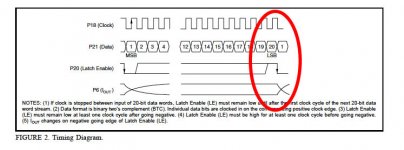
Here, I'm afraid that one is not completely free to choose just any moment for the LE rising edge. There is a clear note about some restraints in the pcm63 data sheet, page 7, figure 2, small letter notes:
In this present scheme of Paul the LE goes up and down totally in between BCLK pulses, so do not satisfy this requirement? For example, if one BCLK is lost in the process, then that would mean only 19 bit's shifted in, and that would explain the level decrease [though it should be 6db?]
Anyway, it's just an observation, might not be relevant. When in doubt, I usually take a digital full scale signal generated, and look at the scope, if the output really swings +/- 2mA ? (or the equivalent after I/V conversion)
Otherways congratulations, Paul, as always!
And thanks to PAOSU, you really found out a neat implementation, I will try it in a similar way!
Ciao, George
First of all, I would like to say wow, nice developments here!
And Paul, thanks for that doc, it is really great!
Though my second thought would be a little bit of doubt.. I had this suspect just before, (and wanted to tell you, Paul) but now that PAOSU had mentioned a possible level change, it just got reinforced.. I had bad experiences with level changes - usually they are the sign of some malfunction.
Here, I'm afraid that one is not completely free to choose just any moment for the LE rising edge. There is a clear note about some restraints in the pcm63 data sheet, page 7, figure 2, small letter notes:
Ok, this is satisfied.If clock is stopped between input of 20-bit data words, Latch Enable (LE) must remain low until after the first clock cycle of the next 20-bit data word stream.
(4) Latch Enable (LE) must be high for at least one clock cycle before going negative
In this present scheme of Paul the LE goes up and down totally in between BCLK pulses, so do not satisfy this requirement? For example, if one BCLK is lost in the process, then that would mean only 19 bit's shifted in, and that would explain the level decrease [though it should be 6db?]
Anyway, it's just an observation, might not be relevant. When in doubt, I usually take a digital full scale signal generated, and look at the scope, if the output really swings +/- 2mA ? (or the equivalent after I/V conversion)
Otherways congratulations, Paul, as always!
And thanks to PAOSU, you really found out a neat implementation, I will try it in a similar way!
Ciao, George
Joseph K said:Though my second thought would be a little bit of doubt.. I had this suspect just before, (and wanted to tell you, Paul) but now that PAOSU had mentioned a possible level change, it just got reinforced.. I had bad experiences with level changes - usually they are the sign of some malfunction.
But, there is no level change It seems to be so! With my second update today (in the CD624 with the new back end, skipping the SPDIF) I measured the level before and after the update and there is no change. The performance of the change is just my impression, which means that the sound is more gentle to me.
In this present scheme of Paul the LE goes up and down totally in between BCLK pulses, so do not satisfy this requirement? For example, if one BCLK is lost in the process, then that would mean only 19 bit's shifted in, and that would explain the level decrease [though it should be 6db?]
The second rule you mentioned, means that the LATCH should be high at least one clock impulse. Also satisfied!!!
Anyway, it's just an observation, might not be relevant. When in doubt, I usually take a digital full scale signal generated, and look at the scope, if the output really swings +/- 2mA ? (or the equivalent after I/V conversion)
This is precisely what I did.
Otherways congratulations, Paul, as always!
And thanks to PAOSU, you really found out a neat implementation.
No thanks at all. It was all your idea!!!
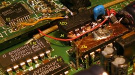
I attach a photograph of the secod update. Much less photogenic.....
Attachments
Dear PAOSU,
Yes, for me this is exactly the point for the remaining little doubt: it is satisfied in time, but not in real clock cycles.. when the clock is stopped, is there anything inside the dac wich still ticks?
But thanks for the clarification about the signal level, because of the number given I thought You have measured the loss.
Anyway, also I had been thinking of it, and had to realize that when having lost one bit of BCLK (19) one looses one LSB, not one MSB, so the loss is much harder to notice.
It is more obvious in the opposite direction, with one BCLK more, (21) then it really halves the amplitude, as I tried to describe earlier.
Anyway, I will do it as well, and report back!
Ciao, George
The second rule you mentioned, means that the LATCH should be high at least one clock impulse. Also satisfied!!!
Yes, for me this is exactly the point for the remaining little doubt: it is satisfied in time, but not in real clock cycles.. when the clock is stopped, is there anything inside the dac wich still ticks?
But thanks for the clarification about the signal level, because of the number given I thought You have measured the loss.
Anyway, also I had been thinking of it, and had to realize that when having lost one bit of BCLK (19) one looses one LSB, not one MSB, so the loss is much harder to notice.
It is more obvious in the opposite direction, with one BCLK more, (21) then it really halves the amplitude, as I tried to describe earlier.
Anyway, I will do it as well, and report back!
Ciao, George
Joseph K said:Dear PAOSU,
Yes, for me this is exactly the point for the remaining little doubt: it is satisfied in time, but not in real clock cycles.. when the clock is stopped, is there anything inside the dac wich still ticks?
There 'ticks nothing' within the DAC. Happily not! Within this time 'everything' comes to rest. No ripples any more, so that when the LE fires (goes down) all is quit and the right value in the register is converted into its analog representation.
In other words, the LE-time is a time, no number of clock impulses. Of course calculating the time is done roughly in a number of clock cycles.
In such specs you will find: 'at least n clock cycles' or 'no more than n clock cycles'. You will NEVER find: 'the length must be (excactly) n clock cycles'.
It is an easy way to define. You see the cycles on the osilloscope so that you can judge easily.
74HC374 or re-re-reclocking LE
Hi guys,
I'm a novice at digital and need some HELP:
On the D1V3 DAC (cs8412 to SM5842 to 74HC86 to PCM63) I have tried a 74HC174 for reclocking LE prior to pcm63 (using CK output from SM5842 as a clock for 74hc) and it has worked well, benefits in more space, detail.
I have now tried a 74HC374 (SM5842 CK was the clock) to reclock LE using the following scheme:
1Q to 2D; 2Q to 3D and 3Q to 4D. I then took the re-re-re clocked LE from 4Q via a 100R resistor to the PCM63.
This sounded MUCH louder than the other channel using 74HC174, and also sounded MUCH more detailed (background sounds much more audible),
BUT at certain points in the music, there would be a loud distortion, like a crackling through the tweeter.
It always occured at exactly the same points in the songs, was there regardless of volume on the pre-amp and seemed to correspond with areas where there was more "energy" in the song.
The only way I found to cure the problem so far, was to take the LE from 2Q to PCM63 and not from 3Q (spiky noise) or 4Q (more spiky noise).
Please help. PS voltage is at 5V, OE is tied to ground. Is there a better chip to use, should I be using some 74HC74's in series or am I missing something here?
PS. The amount of detail being retrieved is AMAZING, now I just need to get rid of those nasty occasional glitches!
Interesting stuff! I too noticed a slight drop in apparent level and similar changes to those which Herb described. Given there is no easy way to a/b it's difficult to be 100% certain regarding the drop in level. I guess measuring the output level for a specific dbFS level would tell you fairly quickly. I had put the difference down to leaner sounding bass.
Joseph K, I see your point regarding the absence of BCLK. Looking closely at the the timing diagram in the PCM63P data sheet (figure 2.) it would seem to indicate LE must be high for one BCLK pulse. While it "works" this obviously isn't what the datasheet calls "correct operation", so it's back to the drawing board to find a "correct operation" solution.
As an interim "hack" AND'ing WCKO and DG would give correct operation and a little more "breathing space" after the falling edge of LE.
Paul
DR H
you have delayed LE by 4 clock cycles. On the rising edge that is no problem, but the falling edge now occurs 2.5 clock cycles after BCLK restarts, and this violates the following.
"(1) If clock is stopped between input of 20-bit data words, Latch Enable (LE) must remain low until after the first clock cycle of the next 20-bit data word stream."
The falling edge triggers the conversion operation so this means you are loading data into the internal dac's after the next word has begun loading into the serial-to-parallel register. Because the BCLK has started running the 2 MSB bits of the original data word are being shifted out of the serial-to-parallel register, and 2 MSB of the following data word are shifted onto the end of the data word as LSB's. So what gets latched into the dacs is a Frankenstein data word. The overall effect is that volume appears to be boosted significantly (x4) but results in any signal that uses the 2 missing MSB being clipped. The 2 lowest bit of the signal is now comprised of the MSBs of the following word.
To get this to work you'll have to delay BCLK and DATA by at least 3 clock cycles.
Again LATCH in PCM63
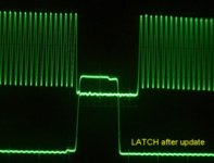
I copied from the NOTES in figure 2: Timing diagram.
(1) If clock is stopped between input of 20-bit data words, Latch Enable (LE) must remain low until after the first clock cycle of the next 20-bit data word stream.
(3) Latch Enable (LE) must remain low at least one clock cycle after going negative.
(4) Latch Enable (LE) must be high for at least one clock cycle before going negative.
(5) IOUT changes on negative going edge of Latch Enable (LE).
My interpretation:
ad.1: LE must remain low (at least) until after the first clock cycle of the next word.
'Remaining low until after the 20th bit of the next word', as in our case, fulfills the rule.
ad.3: In our case the LE remains low for more than 20 cycles, so also this rule has been satisfied.
ad.4: In our case LE remains high for nearly 8 cycles (look at the pictures attached) so this rule has been satisfied.
ad.5: is only a message. It is wise to latch some more time before the first data-cycle of the next word.
All rules has been satisfied.
OK, the rules seems to be more a statute then a technical specification. Luckily I am from a juridical family......
Attachments
spzzzzkt said:DR H
you have delayed LE by 4 clock cycles. On the rising edge that is no problem, but the falling edge now occurs 2.5 clock cycles after BCLK restarts, .....
No,No, NO! Look at my picture of the LATCH (the lower one) and the stopped clock signal. LE falls some 8 cycles before the next word!!!
Mind that the picture itself is not for a stopped clock configuration !!!!
Technicians somtimes are bad writers! Certainly if they are Japanese......
The notes begin with: 'If clock is stopped between....', but this does not mean that the drawing is a stopped clock drawing!
Confusing, yes, I agree.......
FWIW I've attached a diagram of the logic portions of the PCM63P taken from Highton and Murota's AES paper "20bit Colinear DAC, A solution to low level problems".
They refer to another paper (Highton and Ito - An 18-Bit DAC for Consumer Applications) for details of the latch enable:
"In order to minimize chip area a simple latch is used in place of an edge triggered type. This requires on chip generation of a LEC pulse which is achieved with minimal complexity by gating together the word clock and the clock pulse."
Unfortunately they don't specify what the simple gating consists of, so some study will be required to determine which edges are critical.
Attachments
PA0SU said:
No,No, NO! Look at my picture of the LATCH (the lower one) and the stopped clock signal. Le falls some 2.5 cycles before the next word!!!
Herb,it might help if you READ Dr. H's post!!!!!
He is not using the Tent scheme or the mod I suggested. He is using a flip flop to delay LE by 4 clock cycles without any other changes to the D1V3 circuit.
spzzzzkt said:
Herb, it might help if you READ Dr. H's post!!!!!
He is not using the Tent scheme or the mod I suggested. He is using a flip flop to delay LE by 4 clock cycles without any other changes to the D1V3 circuit.
Sorry, gentlemen, sorry! It is so busy at the thread at the moment (and it is rather late here) that I missed Dr.H.
I think I go asleep.......
CUlater.
P.S.: Paul, the word clock is only for recognising left and right. The LATCH is the only signal that commands the DA-conversion. There are DACs which accept coincidences, but this does not break this rule.
Hi Herb,
If you want to quibble with terminology used by members of the design team for the PCM58 and PCM63 that's entirely up to you.
I would point out that in Tent re-clocking schema the WCKO (word clock output) of the SM5842 is connected to Latch Enable pin on the PCM63P.
cheers
Paul
PS I have a feeling Highton and Murota know a thing or two about DAC's
http://www.patentstorm.us/inventors/Frederick_J__Highton/2127056.html
http://www.patentstorm.us/inventors/Toshio_Murota/970359.html
oK this is really clutching at straws 😉
Fred Highton was granted a patent for a level shift serial-to-parallel register in 1987 (US4692641 - see links above). It contains a nice description of the operation of an enable pulse generator circuit. Like I said there is no evidence that this is what is used in the PCM63, but you'd think (hope!!) there is a fair chance the circuit is operationally similar.
with all those disclaimers and cautions out of the way...
"The operation of the enable pulse generator circuit (5) is that the negative edge (160) of the LEC (latch enable control) waveform causes a logical "1" to appear on the conductor (6), thereby producing EN pulse (162). As soon as the CK pulse (161) appears on the conductor (9), the "1" level on conductor (6) is gated via conductor (116) to the reset input R, causing Q output of master-slave flip-flop (111) to return to a "0" level, i.e. causing the EN pulse to return to "0" level. Further clock pulses such as (163) accomplish nothing until a negative-going edge such as (164) occurs on the LEC waveform."
All makes perfect sense. 😀 The patent goes on to describe differential operation, which is just as well seeing the PCM63P uses a differential LE. My theory would be shot to pieces otherwise 😉
So if we apply this to the PCM63P what could be happening with the modification is that the internally generated Latch is left in the High state triggered by the falling edge of LEC(ie pin 20) until CLOCK (pin 18) restarts and resets the internal Latch Enable. BUT thinking about it, this is what happens anyway with the standard configuration. There is no clock running between falling edge of LEC and CLOCK starting up, so the same situation applies - internal LE is high until CLOCK starts up. At least this seems to explain why LEC must stay low until after the first clock cycle of CLOCK.
It's slightly odd that the requirement that LE is high for 1 BCLK cycle is not mentioned in the stopped clock operation section only as footnote to the timing diagram.
To Paul,
Ok, OK, I told you before that I'm no digital expert.... but the idea was that the edges of the LATCH could produce cross talk, so let them fall inbetween the data words. Of course the requirements should be fulfilled at the same time.
With your update proposal both have been established ! Great, no more and no less, and it seems to make sence.
I never had the idea that the developpers of the PCMs are no very clever people. My only statement is (after 40 years research and development, I got the idea) that most technicions cannot write very well, moreover if they are Japanese and their stuff has been translated by translaters who do not know where they are writing about.
Did you ever read the user manual of a Japanese car?
Thanks Paul,
The stuff I'm trying is very simple compared with your efforts.
So if I delayed BCLK and data by 3 clock cyles, you think it would work?
Can I simply then use another 74HC374 to accomplish the reclocking/delaying of those inputs to the DAC?
And can I continue to use CK (pin 9) of SM5842 for the clock input for the '374?
Quick question: I notice that many schemes choose to invert the clock before using it as CK input on flip flops. Why is that?
Dr. H,
I'm just following what's been done before by people like Guido Tent and learning a little as I go along.
Keep in mind that the ideal from a jitter perspective is one gate per package. The more gates clattering away in a package the higher the level of jitter you induce in the signal, so an octal package is not a great idea. You'll be better off using a well bypassed and decoupled 74HC175 for each line. Tie any unused inputs to ground.
4 clock cycles would be better, 3 clocks cycles is the absolute minimum.
Take a look at the timing diagram in the PCM63P datasheet (figure 2). And also grab the SM5847 datasheet - the timing diagrams on page 26 reflect the output of the SM5842 as configured in the D1V3 and are far clearer than anything in the SM5842 datasheet. They should help you work out what is going on.
Inverting the CK means that the timing is shifted by half a clock cycle. This is often enough to compensate for propagation delays.
cheers
Paul
PA0SU said:My only statement is (after 40 years research and development, I got the idea) that most technicions cannot write very well, moreover if they are Japanese and their stuff has been translated by translaters who do not know where they are writing about.
Did you ever read the user manual of a Japanese car?
Herb,
I do understand what you mean. The fact there is a different designation on each chip doesn't help matters either.
I also really appreciate you taking the time to try the mods out. I'm sure I heard a positive difference (even without ESL's) but it's nice to have confirmation of another set of ears.
cheers
Paul
- Home
- Source & Line
- Digital Source
- Reclocking balanced PCM63