I'm not sure. Google turns up a couple of mentions of the idea but no details.
My interest lies in a low-jitter front end for the PCM63P that retails the basic architecture of the Pass D1. As it goes along the links with the D1 get more tenous 😉
I have been looking at the Teddy Regs. I was originally thinking about using Andy Weekes Jung SR's, but I'm concerned about the board space required. I'd been reading the PFM site and had seen the Teddy Reg and your comments here on using them with the PCM63P so have been looking at those as an alternative.
I've been thinking i need to revise the decoupling on the PCM63P - the D1 uses 220uf/0.15uf pairs on each pin, whereas the datasheets indicates use of small value film caps on most. The (AW)JSR may well work better with only small value caps? Guess this will require some testing...
I don't really see the attraction of NOS and asynchronous reclocking to be honest. The beauty of diy audio is that you are free to follow your interests which means for me, at this point in time, SPDIF, digitally controlled VCXO, x8 oversampling, synchronous reclocking, balanced pcm63 and Pass I/V stage.
It seems the main attraction of the DIR9001 is the lower intrinsic jitter figures, which might be a consideration if you are relying on the recovered clock.
If you take a look at page 7 of the CS8412 datasheet ("Clocks and Jitter Attenuation"), you'll see that FSYNC is generated directly from the incoming data-stream rather than divided down from the recovered MCK, so the digital PLL is referencing a sample clock that is "... as spectrally pure as the digital audio source clock for moderate length transmission lines". It seems preferable to be locking to the relatively unprocessed incoming clock rather than the clock generated by the receiver PLL.
The PIC based PLL I've been working on still needs refining, but that requires a PCB rather than strip board. In its current state the PLL reaches an effective loop filter frequency of below 1hz with a couple of minutes, at which point the PLL switches to a low gain "loose lock" mode. I'm looking at using something along the lines of Walt Jung's "ultra low-noise voltage reference" for the PLL dac, and possibly to also to power the VCXO, which should help improve the jitter performance of the PLL.
I've had some off list discussions with Joseph K and I'm going to try out a modified version of the Tent reclocking scheme with the aim of reducing the number of logic gates used. The plan is to implement the reclocking circuits using pico-gates.
nb: not sure what I was thinking with "retails" in the previous post?? Not a good idea to post at 5.30am I guess.
reclocking schema modification
After many email conversations with Joseph K regarding the Tent, Heijligers, et al reclocking schema I've made a small modification which seems to bring positive results.
While the reclocking schema works wonderfully "as is" a question was raised to the effect of "is it really stopped clock operation if the BCLK starts running while the output is still settling?". Using WCLK/LE output of the SM584* results in BCLK restarting 137ns after the falling edge of LE starts the conversion process while the specified settling time of the PCM63P is 200ns. Joseph K made the suggestion that using the DG output would move the falling edge of LE forward by 2 clock cycles giving a total of 308ns before BCLK restarts allowing the output to settle with minimal activity on the chip.
An email from another member containing comments regarding crosstalk caused by LE going high while the 16th bit is loaded from the DF raised the idea of moving the rising edge of LE after ALL 20bits of data have been loaded into the serial to parallel register eliminating this potential source of degradation.
It turns out that the LE which satisfies these requirements can be generated by ANDing the SM5842/7 DG output with the the Qbar output of the 74AC74. The output of this gate replaces the SM5842/7 WCLK.
I'm running a slightly over-complicated 2 gate version of the above rigged in to the FrankenD1V3 and have been quite pleased with the results. Even in this less than optimal setup it seems like there is better resolution of detail and improved imaging. Not a bad result for the addition of a single logic gate.
Re: reclocking schema modification
Gentlemen, thanks for this excellent study!!! I'm working with the 'TentDAC' and measured nearly the same time intervals.
In respect to the specs of the PCM63, the reclocking circuit satisfies. Also I had my doubts about the timing of the LATCH....
I wonder if the 'fast (200 ns) current output (+_2ma)', here called settling time, dictates the LATCH to go low >200 ns before the first intake of the next data word, but it could be better. No cross talk!
The same counts for the upgoing edge of the LATCH which coincides with the down-going edge of the bitclock (at least in my implementations). The data is 'taken in' on the upgoing edge of the clock, so.....
BUT, I agree !! It can't do any harm and it may do some good.
Question: is WCLK the same as WCKO in the specs?
spzzzzkt said:Using WCLK/LE output of the SM584* results in BCLK restarting 137ns after the falling edge of LE starts the conversion process while the specified settling time of the PCM63P is 200ns. Joseph K made the suggestion that using the DG output would move the falling edge of LE forward by 2 clock cycles giving a total of 308ns before BCLK restarts allowing the output to settle with minimal activity on the chip.
An email from another member containing comments regarding crosstalk caused by LE going high while the 16th bit is loaded from the DF raised the idea of moving the rising edge of LE after ALL 20bits of data have been loaded into the serial to parallel register eliminating this potential source of degradation.
It turns out that the LE which satisfies these requirements can be generated by ANDing the SM5842/7 DG output with the the Qbar output of the 74AC74. The output of this gate replaces the SM5842/7 WCLK.
Gentlemen, thanks for this excellent study!!! I'm working with the 'TentDAC' and measured nearly the same time intervals.
In respect to the specs of the PCM63, the reclocking circuit satisfies. Also I had my doubts about the timing of the LATCH....
I wonder if the 'fast (200 ns) current output (+_2ma)', here called settling time, dictates the LATCH to go low >200 ns before the first intake of the next data word, but it could be better. No cross talk!
The same counts for the upgoing edge of the LATCH which coincides with the down-going edge of the bitclock (at least in my implementations). The data is 'taken in' on the upgoing edge of the clock, so.....
BUT, I agree !! It can't do any harm and it may do some good.
Question: is WCLK the same as WCKO in the specs?
Re: Re: reclocking schema modification
Hi Herb,
This was my feeling also. The change in timing does seem to bring some positive gain but my current test setup for the tent schema is probably not the best indicator of it's true impact. I'd be interested in your impressions if you try this mod out.
Yes, WCKO is the correct designation as used in the SM584* datasheets.
cheers
Paul
PA0SU said:
It can't do any harm and it may do some good.
Question: is WCLK the same as WCKO in the specs?
Hi Herb,
This was my feeling also. The change in timing does seem to bring some positive gain but my current test setup for the tent schema is probably not the best indicator of it's true impact. I'd be interested in your impressions if you try this mod out.
Yes, WCKO is the correct designation as used in the SM584* datasheets.
cheers
Paul
Separating Data and Clock reclocking
In the schemes I attach to this posting, the last updates of my CD624-player is presented.
Please pay attention to the U3 and U3a. In the original reclocking circuit of the TentDAC (as I call it) both, clock signals and data have been reclocked in one IC (74HC175). It is well known that the delay in the 75HC175 depends on the voltage on pin 1 and 16: the power supply.
When one looks at this point, the supply-voltage changes with the audio content because the supply current to the Data-ports depends on the audio content!
Ergo, the delay of the clock signals will be infueced by the audio, which introduces audio-related jitter.
The solution (of Henk ten Pierick) is, to use two IC's 75HC175 connected two separated power supply stabilizers.
Attachments
next scheme....
Here is the next scheme.
Question to Spzzzzkt:
Could you exactly point out between which pins of the different IC's the ADD should be connected to delay the upgoing edge of the LATCH, and to which pin its output should be connected? I could find out myself, but I'm an 'analog engineer', and still learning a lot about digital circuits......
Attachments
I'm working on the basis of using single gate packages for all the reclocking. This should minimise crosstalk as far as possible.
Inputs to the AND gate are:
pin 27 of the SM5842 (U2 in your schema)
pin 6 of 74AC74 (U6)
The output replaces the existing LE/WCKO, so might be able to patch it in by lifting the DF end of R23?
best
Paul
Inputs to the AND gate are:
pin 27 of the SM5842 (U2 in your schema)
pin 6 of 74AC74 (U6)
The output replaces the existing LE/WCKO, so might be able to patch it in by lifting the DF end of R23?
best
Paul
spzzzzkt said:I'm working on the basis of using single gate packages for all the reclocking. This should minimise crosstalk as far as possible.
Paul
U6 ==> U4 I think. I found out myself already. Thanks again for this marvellous update!!!
What about the supply to the single gate packages? You should have a separation at least between the data and the clock gates.
I hadn't finalised the power supplies but I'll make sure there are seperate regs for clock and data gate.
I've attached the current state of the reclocking portion of the DAC. While there are clearly better ways of connecting than spdif I have multiple spdif sources so I'm locked into this protocol out of practicality.
U52 - PIC16F818
U53 is a Linear Tech 16bit serial DAC
VCXO is a tent labs item.
The ref of U53 is feed from a Walt Jung design for a buffered low noise reference. As drawn the tent VCXO is powered from second buffered reference of the same design. With the AD797 it should give a noise density of around 1nv/sqrtHz.
While not shown all gates have Guido Tent ferrite/cap decoupling network on the power pins.
cheers
Paul
spzzzzkt said:I've attached the current state of the reclocking portion of the DAC. While there are clearly better ways of connecting than spdif I have multiple spdif sources so I'm locked into this protocol out of practicality.
cheers
Paul
There is something wrong with your picture. I get an empty page....
SPDIF itself is not the problem BUT the recouvering of the clock. A good designed PLL-VCXO will help, but did you ever recognise to skip the VCXO and use the clock from the source? With an extra cable you could take the clock from the transport (if the frequency matches), or whatever, (which should be a very good XO) and lead it to the clock-input of the filter and the reclocking-circuit! (Of cource the PLL-VCXO must be switched off.)
If you make this option switchable (small relais) you could use this option for sources you could/will update, In case of other sources you still could use the PLL-VCXO.....
BTW, the best voltage references I know, are yellow LEDS!
Attachments
Hi Herb,
I've read Paul Winsers article on CD Jitter, http://www.audiocraftersguild.com/AandE/cd-jitter.pdf , which has a slightly similar idea however uses a clock in the Transport.
Not really feasible at the moment as my transport internal clock runs at 16.9344 MHz. It could be done by using a VCXO and XO then switching clock source and system sampling frequency depending on the connection. I'd prefer to keep it relatively simple as this is my first attempt at putting together a dac.
How accurately can you set voltage with the yellow led? I need precisely 4.5V output from the DAC reference as this an important parameter for the PLL.
don't know what happened with that pdf. I'll try uploading again.
Attachments
spzzzzkt said:Hi Herb,
I've read Paul Winsers article on CD Jitter, ..........
Not really feasible at the moment as my transport internal clock runs at 16.9344 MHz.
How accurately can you set voltage with the yellow led? I need precisely 4.5V output from the DAC reference as this an important parameter for the PLL.
don't know what happened with that pdf. I'll try uploading again.
Hi Paul,
Winser starts well in his article, but there must be an oscillator in the transport (at least a VCXO, controlled by the XO in his DAC) beause most powered on transports will be damaged without an oscillator.
If you do not smash on the coax, the jitter-contribution of a cable is ZERO, so there is no reason not to put the XO in the transport.
What really is bad in the article is his oscillator circuit. Read my web site: 14. Reproducible Low noise oscillators.
Yes, different frequencies in transport and DAC is always a problem. Skipping the VCXO is a real great change in audio!
Are you sticked to the transport? Nowerdays one can buy a second hand CD-player for 30 euro (at least in Eindhoven).
I do not understand the 4.5 volt in the PLL. In my PLL is no Vref at all! The voltage is dictated by the correlation between the freq. and the correlated tuning voltage of the VCXO.
You forgot the '2' in the .pdf. DO NOT USE ELCO's in the PLL !!!!
Cheers,
Herb.
Hi Herb,
I've recreated the pdf to make sure there were no problems, so added 2 to the name for "version control". There was a problem with the original pdf.
The transport I'm using is a VRDS-T1 which is getting a bit long in the tooth but works quite well. I'm in no hurry to trade it for a cheap cdp. I also listen to music from my laptop using the SPDIF output of an Echo Audiofire2 to connect to the DAC.
The reason your PLL doesn't have a 4.5V reference is probably because it's quite different to my setup.
Please take a look at this page:
http://www.eijndhoven.net/jos/dac2/index.html
in particular the section "PIC Software PLL for clock recovery". This should explain the way I'm implementing the PLL.
My implementation is slightly different to what Jos has done. I'm using the cs8412 fsync output as that gives a FS clock recovered directly from the SPDIF input signal, rather that the cs8412 PLL. I feel this is better than trying to sync to a clock recovered using a noisy PLL/VCO.
The PIC compares FSYNC and the output of the VCXO and uses the phase error between the two to generate a DAC output code. If there is no error between the two inputs no output is generated. The 4.5V reference gives the DAC a 0-4.5V output range which matches the input range of the Tent VCXO. This arrangement allows the control voltage of the VCXO to be adjusted in 0.035hz increments.
Once the PLL locks with no error for 1 second the PLL switches into a loose lock mode, which allows the loop to drift within the range allowed by the jitter free mode of the SM5842.
The big advantage to using software driven PLL is that you can get a fairly fast lock, then drop the effective loop filter frequency down to well below 1hz - I'm getting down to at least 0.5hz in the current configuration. This means that incoming jitter is attenuated quite significantly. And no need for elko's in the PLL.
This arrangement seems to offer an improvement over the more standard VCXO setups. Joseph K has implemented a somewhat different implementation of this kind of PLL in his Tent DAC and found that it made an improvement.
cheers
Paul
I've recreated the pdf to make sure there were no problems, so added 2 to the name for "version control". There was a problem with the original pdf.
The transport I'm using is a VRDS-T1 which is getting a bit long in the tooth but works quite well. I'm in no hurry to trade it for a cheap cdp. I also listen to music from my laptop using the SPDIF output of an Echo Audiofire2 to connect to the DAC.
The reason your PLL doesn't have a 4.5V reference is probably because it's quite different to my setup.
Please take a look at this page:
http://www.eijndhoven.net/jos/dac2/index.html
in particular the section "PIC Software PLL for clock recovery". This should explain the way I'm implementing the PLL.
My implementation is slightly different to what Jos has done. I'm using the cs8412 fsync output as that gives a FS clock recovered directly from the SPDIF input signal, rather that the cs8412 PLL. I feel this is better than trying to sync to a clock recovered using a noisy PLL/VCO.
The PIC compares FSYNC and the output of the VCXO and uses the phase error between the two to generate a DAC output code. If there is no error between the two inputs no output is generated. The 4.5V reference gives the DAC a 0-4.5V output range which matches the input range of the Tent VCXO. This arrangement allows the control voltage of the VCXO to be adjusted in 0.035hz increments.
Once the PLL locks with no error for 1 second the PLL switches into a loose lock mode, which allows the loop to drift within the range allowed by the jitter free mode of the SM5842.
Jitter-free mode (SYNCN = HIGH)
When SYNCN is HIGH, the timing error value is ±3/8 * (LRCI clock period). When the difference between the input timing and LRCI start edge position do not exceed this value, internal timing is not resynchronized and all functions continue to operate normally.
The big advantage to using software driven PLL is that you can get a fairly fast lock, then drop the effective loop filter frequency down to well below 1hz - I'm getting down to at least 0.5hz in the current configuration. This means that incoming jitter is attenuated quite significantly. And no need for elko's in the PLL.
This arrangement seems to offer an improvement over the more standard VCXO setups. Joseph K has implemented a somewhat different implementation of this kind of PLL in his Tent DAC and found that it made an improvement.
cheers
Paul
spzzzzkt said:Hi Herb,
The reason your PLL doesn't have a 4.5V reference is probably because it's quite different to my setup.
Please take a look at this page:
http://www.eijndhoven.net/jos/dac2/index.html
cheers
Paul
I used an obsolete HEF 4750 as in all my radio-applications. It has two loops: frequency comparison (for the fast locking) and phase comparison. There seems to be a successor, but the solution of Jos (I know him very well) is better I think.
I'm not sure about any receiver output. I do not trust them. I have built me a direct conversion receiver for phase noise measurements. It is amasing how bad most sofisticated circuits are in this field...... Even many XO's (not those of TentLabs) are bad. I developed my own XO which is very good. See the attachment.
Stabilisation is best done with a couple of LEDs in series. The red, yellow, green and whatever, all do have a different operating voltage. The red ones are the most temperature stable. It is rather simple to select them with a digital multi-meter.....
Attachments
LATCH update
I will show you the update in the TentDAC (as I call it) with a simple ADD which has been discussed about eight replies before. Luckily the connections to be made are close to each other. It is a pitty that I cannot show the three pictures in one reply.
Here is 'the old' situation. The LATCH on the PCM goes high just before the 16-th bit of the DATA and goes down (the LATCH-function) only 136 ns before the next data-intake.
Attachments

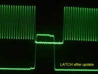
LATCH update
Here is the picture after the update with a simple ADD-function as described by Paul above.
The LATCH goes high after the last (20-th) bit and goes down two clock cycles earlier.
This is theoratical mutch better. I do not know jet if it is audible. I just finnished it.
Here is the picture after the update with a simple ADD-function as described by Paul above.
The LATCH goes high after the last (20-th) bit and goes down two clock cycles earlier.
This is theoratical mutch better. I do not know jet if it is audible. I just finnished it.
Attachments
LATCH update
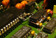
Last but not least I will show you how simple the soldering is.
I fixed 'the ADD' (74HC08) on top of U4. An earth screen between them. P4 end P5 are the inputs, P6 the output.
I lifted P25 (WCKO) of the dig.filter (SM5842AP) and put a wire in the whole of P25 and connected the other side to P6 of the ADD.
With a 100 ohm resitor the connction between Qbar (P6) of the underlaying U4 and P4 of the ADD has been made.
With a 100 ohm resitor the connction between DG (P27) of the dig.filter and P5 of the ADD has been established.
All connections are very short!
The photograph attached here, makes all clear.
Attachments
Nice work Herb!!!
I'm too embarrassed by the rats nest of wire in the D1V3 to post pics The mod should work better when the underlying reclocking schema is already properly implemented, so you should hear clearly what difference the modification makes.
Look forward to your report on listening tests.
cheers
Paul
I'm too embarrassed by the rats nest of wire in the D1V3 to post pics
The mod should work better when the underlying reclocking schema is already properly implemented, so you should hear clearly what difference the modification makes.Look forward to your report on listening tests.
cheers
Paul
- Home
- Source & Line
- Digital Source
- Reclocking balanced PCM63