I can also try to solder the opamp directly on the PCB but I don't think it comes from there since I have the same thing on the Q17-Mini.
Hello!
I tried with opamp soldered on the back on the SMD footprint.
No change.
Stef.
Hello Stef,HI Tim!
I tried the filter circuit on R6. No change at all.
Still 34mV of DC offset and 11MHz sinus...
Cheers,
Stef.
that's unfortunate that this filter is of no use. I have simulated a few more things, but I can't come up with a favourable result, which is why it's worth heating up the soldering iron.
Actually, it would be a test to build up Tibi's original for comparison so that there is a reference and then compare on that basis. I have also thought about building up Tibi's original on his current board and starting a comparison, but admittedly this is no small effort and I have prejudices about the output resistance implemented in the original, which I have found to be too high in past tests. In addition, there are the expensive components from the USA, which I don't need in my set-up.
Maybe you can come up with a variant, it is not easy to modify this especially optimised amplifier.
Regards Tim
@stef1777
Please keep current dumping bridge away from cascode stage.
Start your design putting down circuit requirements first.
@Hennady Kovalsky
You want to say gate voltage compensation.
As I already mentioned, output stage run in class B and the current through output stage is negligible.
CCS made with Q12 and Q6 will push a current trough R11 respectively R12 that will lift output stage Vgs near Vgstheshold.
As soon the amplifier start to operate, output transistors will start to dissipate power, their Vgsth will drop, transconductance increase and output stage will start to operate more and more in class A/B. To avoid this I make use of Q12 thermal run to compensate.
Regards,
Tibi
@stef1777
Please keep current dumping bridge away from cascode stage.
Start your design putting down circuit requirements first.
Tibi
Hi Tibi,
Can you be more specific?
Stef.
Hello!
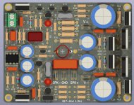
I built the prototype of Q17-P2. At first sight, the card works but it oscillates alas. This is the sinus with see on the scope screenshot below.
I have 35mV of offset at the output with the voltmeter connected directly to the HP terminals. More if I connect an 8R load connected with the scope.
Nothing is very hot.
I have to find where it comes from which is not an easy task. 😆
Stef.

By having such huge distance between n and p output finals, you add an important parasitic inductance that may alter current dumping bridge operation and induce in all PCB lot of signal from output.
Regards,
Tibi

So if I understand correctly. My idea of putting the N and P channel at each end of the PCB will never work?
The objective of my idea was to have a board that was not very wide so that the card would fit in a box that was not very high.
Stef.
The objective of my idea was to have a board that was not very wide so that the card would fit in a box that was not very high.
Stef.
1. Keep current dumping bridge away from other small signal traces.Hi Tibi,
Can you be more specific?
Stef.
2. coil must be away from cascode
3. use gnd plane and guard, where possible, small signal traces
4. tight placement of output stage with thick traces.
5. keep some space between output transistors and class A stage made with Q5 and Q6
6. avoid pcb islands not connected
7. gate stoppers must be as close as possible to gate mosfet pin
8. keep decoupling caps as close to mosfet drain or opamp pins.
Regards,
Tibi
I think there are far better ways to make a very good pcb for Q17. ;-)So if I understand correctly. My idea of putting the N and P channel at each end of the PCB will never work?
The objective of my idea was to have a board that was not very wide so that the card would fit in a box that was not very high.
Stef.
Regards,
Tibi
Absolutely right you said!By having such huge distance between n and p output finals, you add an important parasitic inductance that may alter current dumping bridge operation and induce in all PCB lot of signal from output.
Regards,
Tibi

Apparently, dead end for this P2 project.
Would you have an idea to make a narrow PCB so that it fits in a low cabinet?
Stef.
Would you have an idea to make a narrow PCB so that it fits in a low cabinet?
Stef.
Stef, why won't you use tvicol's board, mounting them horizontally with 90° transistors on an inside sink?
I'm pretty sure it'll fit in a 2U mini Dissipante.
I'm pretty sure it'll fit in a 2U mini Dissipante.
Stef, why won't you use tvicol's board, mounting them horizontally with 90° transistors on an inside sink?
I'm pretty sure it'll fit in a 2U mini Dissipante.
Hi G600,
I have already thought about this method but it takes up a lot of space in the box and does not leave much room for the rest.
Regards,
Stef.
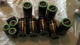
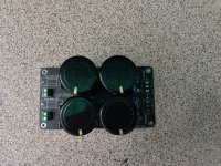
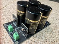
Mundorf MLytic. 2200uF/63V will fit on Q17 pcb and 15.000uF/63V will fit perfectly on active power supply pcb.
- on bard filter capacitors have been increased to 4700uF. I think this is maximum value for this footprint. In terms of sound, this caps matter a lot, so you may voice your amplifier by changing them.
Is there a recommandation for this capacitor with a lifespan of more than 2000 hours?
Thanks.
Regards,
Tibi
Attachments
Unfortunately, you misunderstood me, it meant that the compensation bridge when using mosfets in the output stage does not justify itself, since the driver stage, instead of pumping the input capacitance of the output transistors, is loaded through a direct connection resistor to a low load ...@Hennady Kovalsky
You want to say gate voltage compensation.
As I already mentioned, output stage run in class B and the current through output stage is negligible.
CCS made with Q12 and Q6 will push a current trough R11 respectively R12 that will lift output stage Vgs near Vgstheshold.
As soon the amplifier start to operate, output transistors will start to dissipate power, their Vgsth will drop, transconductance increase and output stage will start to operate more and more in class A/B. To avoid this I make use of Q12 thermal run to compensate.
Regards,
Tibi
For your circuit, the optimal initial current is 80mA, the feed-forward resistor from the bridge should be removed, the remaining components should be adjusted according to the stability of the circuit and the capacitive load according to the Boucher equation - then you will have an audiophile quality of the circuit....
Black used feed-forward compensation for an output stage with a cutoff angle of less than 90 degrees, this is not even class B but class C. The quasi-complementary output stage generated even harmonics, which masked the distortion of the output stage curve. Now is not 1970, now the quality of components is much better.
Mosfets have no switching distortion, they do not need to be compensated ...everything is decided by setting the optimal initial current.
Last edited:
@Hennady Kovalsky
Thank you for your comments.
You are right, class A stage (the driver) is not best loaded. I'll address this in a high power future version.
I'll make some simulations with 80mA. I think you refer to driver stage. Howdo you get this value ?
Regards,
Tibi
Thank you for your comments.
You are right, class A stage (the driver) is not best loaded. I'll address this in a high power future version.
I'll make some simulations with 80mA. I think you refer to driver stage. Howdo you get this value ?
Regards,
Tibi
Thanks, what do you think is rational.@Hennady Kovalsky
Thank you for your comments.
You are right, class A stage (the driver) is not best loaded. I'll address this in a high power future version.
I'll make some simulations with 80mA. I think you refer to driver stage. Howdo you get this value ?
Regards,
Tibi
80mA is the current of the output transistors, 40-50mA is enough for the driver.
I have something in mind that will use lateral mosfet's in output stage.
These will run in A/B biased at ~80-100mA
Regards,
Tibi
These will run in A/B biased at ~80-100mA
Regards,
Tibi
HI!
Let me know if you modify the circuit. As I have finished my stock of Q17-Mini 1.2 PCB, I am working on a new 1.3 version with some changes to the PCB (moved Q8 close to Q7). I can incorporate changes if you want with the first batch.
Regards,
Stef.
EDIT: I finally found the time to compare the OPA1641 and OPA1611 with the Q17-Mini. I prefer the OPA1611. This softens the sound a bit.
Attachments
Last edited:
- Home
- Amplifiers
- Solid State
- Q17 - an audiophile approach to perfect sound