When the amp is cold (not powered up) I see the output resistance between the speaker connectors as 0 ohm and the input resistance as 20k ohm. Do you want me to check when its powered up too?
I checked each leg of the transistors for shorting using the DMM and all seems to be good. Nothing has broken as I used a bulb tester for the new board to test. I have also removed the board from the heat sink and tested with the same results.The transistor is broken
Last edited:
One of my PCB versions have output connector reversed and is in short. Please measure the other pcb you have not mounted yet and send me macro picture with top and bottom pcb zone where output connector is.
Regards,
Tibi
Regards,
Tibi
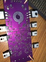
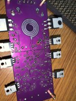
I have mounted all the parts on the other pcb too but not the output connector. I have checked the output connectors both ways and it still shows 0 ohms. Let me share a pic


Attachments
Last edited:
Yes, this is the issue. It was long corrected, but unfortunately you picked exactly this version and put in production. Sorry for this.
Here is what you can do.
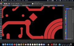
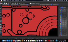
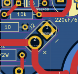
As you can see both output's, round + and square - , are connected to power ground.
The round one should be disconnected from ground. For this you need to cut thermal traces as in attached picture. Use a sharp cutter and after that measure, to be sure that output is no longer 0 ohm.
Regards,
Tibi
Here is what you can do.
As you can see both output's, round + and square - , are connected to power ground.
The round one should be disconnected from ground. For this you need to cut thermal traces as in attached picture. Use a sharp cutter and after that measure, to be sure that output is no longer 0 ohm.
Regards,
Tibi
Attachments


Good news @tvicol I did the trace cut as you suggested on the new board and checked the resistance between the circle pad and the dc ground, it was 650 ohms. Is the output ground isolated in your design as I do not see any resistance between this and the output signal even with 2/20M on my DMM. Now powered up this amp board with the bulb tester and it works fine with glowing and then immediately getting completely switched off 🙂
Removed the bulb tester and powered up directly amp works fine with the offset being around 0.01-0.05mV but need to check the bias around the 47/1w resistors both sides to measure. Will do a full test later tonight and also make a listen to this channel.
And the bad news my first amp board seems to have toasted the big mosfets as they show continuity on my DMM for all the 3 legs. Or because the output connector is soldered its giving this not sure. I need to first desolder the output connector and check for the continuity of the mosfets and if its exist then need to change them 🙁
Thanks
Hello!I built a mini version. And it ran without any problems. I will test it under load.
View attachment 1027902
View attachment 1027901
Nice. How much DC offset at output do you have?
Stef.
Good observation. As it is, the square output is not connected to anything, so you need to connect square connector to output power ground.... Is the output ground isolated in your design as I do not see any resistance between this and the output signal even with 2/20M on my DMM. ...
I suggest you that, on bottom, to make a short wire trace between square output connector and power ground plane.
Than power the module and measure DC offset.
Regards,
Tibi
Last edited by a moderator:
0,038V, But that's without warming up. The board is still without a heatsink.
The offset will not move much even when hot. You can manage to lower it a little bit by sorting Q1, Q4, R10, R13 and R32.
I managed to get it down to 34mV by doing this on my current 1.1 board.
I can't wait to see if I managed to lower the offset a bit with the new PCB design of my Q17-Mini 1.2 board. Still waiting for it...
Regards,
Stef.
Curiously Tibi I actually downloaded the Q17 gerbers from the Github the latest ones last month when I printed them. So not sure if the gerbers on your Github are the latest or did you change and updated it recently? Please change if not in the Github that others like do not get into the confusion that everything is good but the amp does not work 🙂Yes, this is the issue. It was long corrected, but unfortunately you picked exactly this version and put in production. Sorry for this.
Here is what you can do.
As you can see both output's, round + and square - , are connected to power ground.
The round one should be disconnected from ground. For this you need to cut thermal traces as in attached picture. Use a sharp cutter and after that measure, to be sure that output is no longer 0 ohm.
Regards,
Tibi
Thanks again for the help.
Gerbers on GitHub are OK (see attachments) and the ones on this thread (first post) have been updated recently.
As I said, you have downloaded a previous version where, somehow, I reversed output connector. My bad and I apologise for this ... 🙁
Regards,
Tibi
As I said, you have downloaded a previous version where, somehow, I reversed output connector. My bad and I apologise for this ... 🙁
Regards,
Tibi
Attachments


It works just as well with the LM49710. The tweeter is a bit bigger. Here the Opus can be used as an equalizer ))
Thanks Tibi, maybe I downloaded the previous version and uploaded the same to the JLCPCB site for printing 🙁Gerbers on GitHub are OK (see attachments) and the ones on this thread (first post) have been updated recently.
As I said, you have downloaded a previous version where, somehow, I reversed output connector. My bad and I apologise for this ... 🙁
Regards,
Tibi
Also can you also please confirm the polarity on the input signal socket which is the hot signal side and the signal ground as the confusion is with the small "Arrow" symbol near one of the pads?
- Home
- Amplifiers
- Solid State
- Q17 - an audiophile approach to perfect sound