
With normal MKP, I have a vapourised polypropylene film..........................
Tim, thank you for your detailed explanation; did not realise any of this.
I have a few Audyn KP Sn which appear remarkably heavy. Soundwise... certainly different but cannot say i am too impressed.
Waspaudio/KDMaudio/Julien :Hi to all !
Firstly I have to say thanks to Tibi for sharing his design
Secondly, congrats to everyone regarding their results so far.
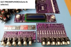
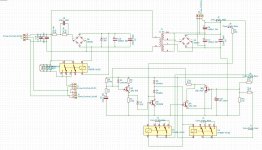
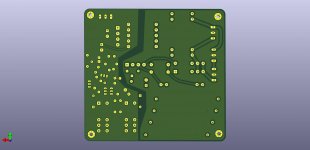
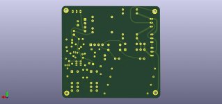
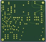
Last but not least, may I present my version of the Q17 pcb.
Should start assembling soon !
Regards
Your pcb project is beautifull .
Tnx !
I'm not surprised that the kpsn don't impress you. For me, they are the most neutral capacitors I know. When developing loudspeakers, I use them for the mid- and high frequencies, because then distortions, frequency response errors and phase jumps can be heard very well and the potential of the loudspeakers can be recognised very quickly. In order to build inexpensive speakers, the quality of the capacitors is then reduced, frequency response and phase errors are built in very discreetly until the sound is right. That's why the kpsn is also branded with "harsh" sound, which is not audible with normal capacitors.
I have also compared kpsn with gold silver MKP, where the kpsn is also more detailed - rather a little more - but the other can convey a much softer sound, so the sound is softened quite ideally.
In many cases, that sounds more pleasant.
I have also compared kpsn with gold silver MKP, where the kpsn is also more detailed - rather a little more - but the other can convey a much softer sound, so the sound is softened quite ideally.
In many cases, that sounds more pleasant.
Hello,
And my PCBs are ready!
I am waiting for a series of electronic components and accessories and next week I will prepare them for tests.
I am referring strictly to amplification modules.
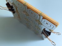
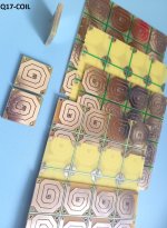
I am happy in this way to present you my innovative coil 🙂).
It has 4 layers of 70u and only 25x25x3.8mm.
I'll be back with more details after the tests!
I hope time allows me next week ...!
And my PCBs are ready!
I am waiting for a series of electronic components and accessories and next week I will prepare them for tests.
I am referring strictly to amplification modules.
I am happy in this way to present you my innovative coil 🙂).
It has 4 layers of 70u and only 25x25x3.8mm.
I'll be back with more details after the tests!
I hope time allows me next week ...!
Attachments
-
 Q17-PRE.jpg503.4 KB · Views: 371
 -
 Q17-ACC.jpg384.6 KB · Views: 314
 -
 Q17-SUPPLY.jpg574.3 KB · Views: 284
 -
 Q17-CROWBAR.jpg404.5 KB · Views: 327
 -
 Q17-COIL2.jpg135.3 KB · Views: 342
 -
 Q17-COIL.jpg439.8 KB · Views: 330
 -
 Q17-3P1.jpg536.1 KB · Views: 562
 -
 Q17-3P.jpg557.8 KB · Views: 551
 -
 Q17-1P-B.jpg553.1 KB · Views: 571
 -
 Q17-1P.jpg556 KB · Views: 603
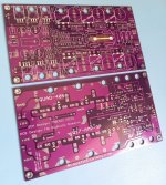
Hello,
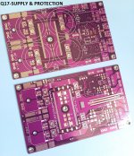
for my power version of the Q17 I have now combined the switch-on delay and speaker protection circuit on one board. It is the circuit here from the forum / store, which I have slightly modified. Strictly speaking, I replaced the flashing light by a permanently glowing LED, and added an additional power output for an electric radio potentiometer.
I assume that it should work like this, however I can't estimate exactly if the travo with its rated voltage of 2x 9V is sufficient. However, it is the case that these transformers tend to have a higher output voltage, so I suspect that the necessary 25V DC to switch the two relays will be achieved.
Regards Tim
Attachments
I have used the following:
https://www.diyaudio.com/media/build-guides/diyaudio-softstart-build-guide-v1.0.pdf
and:
Speaker Turn On Delay and DC Protector Board Set (V3)
I don't need a protection circuit for stupid people who operate the amplifier in short circuit until smoke rises. The switch-on delay is a must due to the transient of the amplifier, because it sounds very bad. The DC protection kicks in when the amp is broken and the main fuse kicks in when the transformer is broken.
Last edited:
Congratulations on the initiative, Tim!
But I have a series of suggestions for you, for your safety!
1. It is mandatory to separate the two functional modules on different PCBs for electrical safety reasons.
2. You must keep in mind that from the routes that carry the voltage of 220Vac to the chassis or to the metal parts in human contact you must have a distance of at least 5-6 mm if the chassis or metal parts are connected to earth.
3. Between the primary transformer powered at 220Vac and the secondary transformer, you must have at least 7-8 mm of insulation space!
Hello sorinsistem,
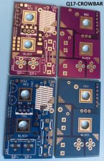
It's true, I didn't place the contacts between low voltage and high voltage optimally, I've scaled that to 6mm now. Also the note to the earth is good, so I have the two mounting holes in the high voltage area also connected to earth and increased the distance to the last power resistor. It is now certainly not so super that all standards are met with it, but already significantly better than what you find in switching power supplies.
It's true, I didn't place the contacts between low voltage and high voltage optimally, I've scaled that to 6mm now. Also the note to the earth is good, so I have the two mounting holes in the high voltage area also connected to earth and increased the distance to the last power resistor. It is now certainly not so super that all standards are met with it, but already significantly better than what you find in switching power supplies.
Attachments
It is ok now to isolate between primary and secondary, but give up the ground plan which can create very big problems in practice ... The ground plan is used in audio or radio applications where you work with very low intensity signals ... It has nothing to look for ground plan in high voltage applications ... Favor the contouring of high voltage lines ...
And we are not talking about the observance or non-observance of some norms but about the functionality of your work ...!
I'm sure you don't want to work in vain!
And we are not talking about the observance or non-observance of some norms but about the functionality of your work ...!
I'm sure you don't want to work in vain!
You mean surfaces against ground or housing GND are unfavorable?
The other surface is only a (-) voltage surface of the switching voltage of the relay, which works independently of whether it is designed as a conductor track or surface, so or otherwise without relevant electromagnetic effects (my opinion).
In your opinion, is the following layout more suitable for minimizing electromagnetic radiation?
Attachments

It's all much, much better!
I would give up the "PE" connection on the PCB. This connection can be made to a screw fixed to the chassis! It is practically not necessary on the PCB ...!
Success!
I would give up the "PE" connection on the PCB. This connection can be made to a screw fixed to the chassis! It is practically not necessary on the PCB ...!
Success!
sorinsistem1 said:It's all much, much better!
I would give up the "PE" connection on the PCB. This connection can be made to a screw fixed to the chassis! It is practically not necessary on the PCB ...!
Success!
If so, I have another variant with 9V output here. I still have a motor-driven potentiometer ( ALPS27 motor potentiometer Remote control volume potentiometer board Double 10K 50K 100K For Audio POWER amplifier NEW|Instrument Parts & Accessories| - AliExpress ), which actually only needs 5V, but it has its own regulator on the board. An additional 7809 is just a sharing of the power dissipation to several devices, nothing more.
Attachments
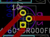
Maybe Q12 needs to be reviewed. If it is positioned properly in PCBNew as told in the documentation to be mounted on the backside (acting as thermal compensation) the pinout is obviously flipped. PCBNew is telling you that too, if you configure the footprint the right way.
I can see in your pictures, that you're mounting it like told in the documentation, but then the schematic isn't right anymore because pin 1+3 are switching positions when mounted on the backside.
What is right now? Are you switching the pinouts "hardwired" under the board again?
I can see in your pictures, that you're mounting it like told in the documentation, but then the schematic isn't right anymore because pin 1+3 are switching positions when mounted on the backside.
What is right now? Are you switching the pinouts "hardwired" under the board again?
Attachments

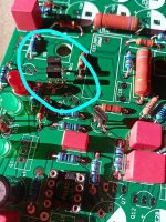
The very first PCB had many design faults. If you look close into the pictures, you may notice that all small transistors are mounted reversed.
Don't guide yourself looking at pictures, instead use KiCad 3d.
Later on, all these problems have been corrected, so the files from github are 4th iteration.
About your observation, you are right and that's why KiCad source files are available. Correct and make a better PCB.
In the prototype, Q12 is mounted near final stage with wires.
Regards,
Tibi
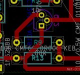
Thank you. So assuming the symbol in the schematic is correct I switched then position of R19+R13 for painless routing to the now flipped Q12. Maybe this is something you could implement too for one possible source of human fault less? When builders see "Oh, there is a silkscreen marking on the backside? Better read the manual again to see what its doing!" When it's routed correctly there's a point of possible confusion avoided, too  .
.
.Attachments
Last edited:
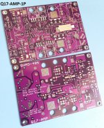
One more detail about the small MosFET:
I based my layouts on the pinout of the first variant of Tibi schematic, so there are also the markings to drain and source on my boards. Practically the P-channel models are installed reversed in the E-line case.
I based my layouts on the pinout of the first variant of Tibi schematic, so there are also the markings to drain and source on my boards. Practically the P-channel models are installed reversed in the E-line case.
Attachments
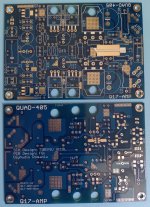
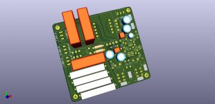
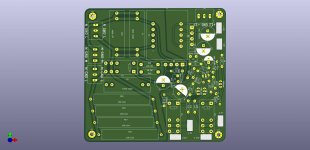
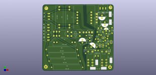
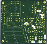
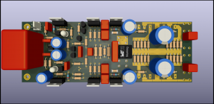
Something about my version of the PCB for the Q17...
I'm using surface mount coils in my designs. For me it's worth it - and I don't have to bother about selfmade coils...
High-current paths are without solder mask so they could be filled with solder or copper could be soldered on them. Source resistors are splited into five 1W types so the paths are shorter and it looks tidier.
Attachments
Last edited:
- Home
- Amplifiers
- Solid State
- Q17 - an audiophile approach to perfect sound