Hi TimHello everyone,
I would like to discuss the recent changes to the Q17 and derive ideas for optimization. Originally, a current mirror was formed with Q9 and Q11, with its input current depending on Q12 and R24+R25, regulating the current for the cascode. Thus, it was a feedback correction. The variant from this summer (by Tibi), accurately reproduced by Stef, changed this by replacing the simple current mirror with a Wilson current mirror.
So far, nothing new.
Now, this Wilson current mirror has an impact on the current for the cascode and the currents in the circuit of Q5+Q6. Therefore, it is understandable that Tibi reduced the resistors R10 and R13 to 9.1 ohms. However, the adjustment of R3 is missing. In the original concept with a simple current mirror, R3 was chosen quite ideally at 150 ohms. In the concept with the Wilson current mirror, this value needs to be reduced to the order of 100 ohms for the circuit to work well-balanced again.
Since the circuit is a Class A feedback correction with Q5 and Q6, generating higher impulses when driving two pairs of Mosfets (Q15, Q16, Q17, and Q18 - in Stef's Turbo), there is increased instability in terms of oscillation behavior. I've dampened the oscillation behavior a bit by adding a resistor (R34) to C10 – this suggests that the mica capacitor without a resistor is not perfect (I can demonstrate this in the Spice simulation) and that a high-frequency capacitor with high ESR – like the cheap ceramic capacitors – would be more suitable in this position.
Additionally, I'm damping high-frequency oscillations of the feedback path (Q12 – R24+R25) by adding an additional damping element (R35 + C20) compared to the central feedback (through R27).
Now, in this context, I have determined that R3 is still too high in my latest version (#2,204) and should be adjusted.
During these investigations, I explored the question of which alternatives to Q12 can have a positive influence. In the simulation, I picked up the possibility of 2N5551 and found a solution with a high base resistor (R9). Since I want to keep the quality of the components as high as possible, I chose the ZTX458 as an alternative to 2N5551 (as Q12). As the simulation of the Wilson current mirror behaves little positively compared to the simple current mirror, I also simulated a double current mirror with P-MosFET. Now there is the idea of building all components of the Wilson current mirror, including Q10, with ZTX558. This results in a simulation result that is even more precise than with P-Mosfets.
This adjustment allows a lowering of resistors R11 and R12, making the power stage in Class B almost error-free at the zero crossing.
The reason for this investigation is provided by the Hafer interpretation: https://www.diyaudio.com/community/threads/unusual-amp-from-1987.357369/post-7493521
In this amplifier, the Class B power stage also works very precisely, which the Q17 in its current form does not. However, the described circuit works with extremely small signals, which reduces my enthusiasm. Therefore, I consider it more promising to further optimize the Q17 circuit.
What do you think?
Best regards, Tim
When wil we see a board layout of this, as I would like to build it.
Kind Regards
I have simulated the Turbo 1.2 using the alternative MosFET spice models Q5 FQPF7P20 and Q6 2SK3564, and I cannot identify any anomalies in the simulation. Therefore, I can't immediately think of what could be "defective" in your case.Hello!
Thanks for the tip, I noticed that too and have already replaced it. Unfortunately the same error still occurs
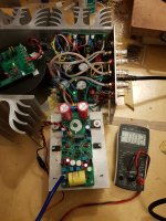
I've desoldered almost all parts and soldered those at a new pcb.
Indeed, it works. I hooked it up with a test sepaker and it sounded as well.
The dc offset is -0.2mV.
But it arises to -3.5V in about 10sec after turning off.
Is this normal and acceptable?
Indeed, it works. I hooked it up with a test sepaker and it sounded as well.
The dc offset is -0.2mV.
But it arises to -3.5V in about 10sec after turning off.
Is this normal and acceptable?
Attachments
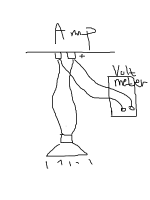
This is like a leftover charge that is asymmetrical. Therefore, you need a load resistor or a small loudspeaker for this measurement, then you can determine how large this charge really is.

try the same procedure with RCA input shorted.I've desoldered almost all parts and soldered those at a new pcb.
Indeed, it works. I hooked it up with a test sepaker and it sounded as well.
The dc offset is -0.2mV.
But it arises to -3.5V in about 10sec after turning off.
Is this normal and acceptable?
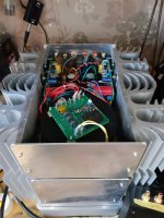
I have an issue of cross channel ground loop.
It has made so BIG hum.
I've changed 0R0 to 10R0 of R32 (HBR).
It made hum smaller but hum still has been remained.
I've made closer RCA connectors and connected RCA grounds.
The hum is gone!!
@poseidonsvoice
Thank you for sharing this document.
https://hifisonix.com/wp-content/uploads/2019/02/Ground-Loops.pdf
Attachments
hiI've desoldered almost all parts and soldered those at a new pcb.
Indeed, it works. I hooked it up with a test sepaker and it sounded as well.
The dc offset is -0.2mV.
But it arises to -3.5V in about 10sec after turning off.
Is this normal and acceptable?
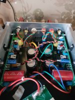
at post 2223 where goes the RCA input? the GND from the RCA goes...cant see it
edit:
the other pics are clear. check if you have tight contact with all earth connections...check solders and crimp connection
Hi Nam,
You should take away the earth connection between Signal-input L and R. (the two RCA's)
Start enjoying your music!
You should take away the earth connection between Signal-input L and R. (the two RCA's)
Start enjoying your music!
Hi Alex,Hi,
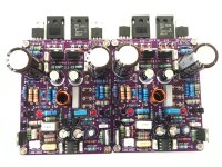
A small contribution to this project. PCB is not tested, maybe there are errors, maybe someone will check. If all goes well, I'll make the Gerber file available. I have always liked Quad and I made some copies. I'm posting some pictures.
I like your project very much. You said that if it works then you'll make the Gerber files available. Did you tested ? Can you send me the files or just the simple converted versions of the front and back PCB ? preferably without non copper layers, as I can see them in your post
Is there any problem of connecting grounds of L / R signal ?Hi Nam,
You should take away the earth connection between Signal-input L and R. (the two RCA's)
Start enjoying your music!
I have just followed the guide of the doc and it made hum gone.
Nam!
Left and right are separated units. When built following Tibi's diagram there should be zero hum! Using R32/10 Ohm will give about 35mV offset, strapped makes about zero offset. Both ways: no hum!
Left and right are separated units. When built following Tibi's diagram there should be zero hum! Using R32/10 Ohm will give about 35mV offset, strapped makes about zero offset. Both ways: no hum!
I've changed the R32 (HBR) from 10R to 1.8R.
It makes about 3mV dc offset.
I'm using 83db low sensitivity speaker.
The 1.8R is sufficient to remove hum and it makes sound softer and better transient than 10R.
I guess that the higher dc offset makes sound harder and more compressed.
It makes about 3mV dc offset.
I'm using 83db low sensitivity speaker.
The 1.8R is sufficient to remove hum and it makes sound softer and better transient than 10R.
I guess that the higher dc offset makes sound harder and more compressed.
Hi namgiwook
sorry...but i do not understand what you are doing and what should be a DC offset to do with your problem and oes this to the sound.
sorry
i am out...
sorry...but i do not understand what you are doing and what should be a DC offset to do with your problem and oes this to the sound.
sorry
i am out...
Please tell us more what changes have you made? I am soon planning to build one.I have optimized my design for the Q17 turbo...
I've changed the R32 (HBR) from 10R to 1.8R.
It makes about 3mV dc offset.
I'm using 83db low sensitivity speaker.
The 1.8R is sufficient to remove hum and it makes sound softer and better transient than 10R.
I guess that the higher dc offset makes sound harder and more compressed.
Hello Namghiwook,
I am trying to explain the effects of the R32 modification:
Firstly, the DC offset is a result of the current flowing through R6, which is the current from the positive side through the cascode to ground. R32 is a resistor where a voltage drops, causing an increase in the Input GND by this amount. Since the amplifier is controlled by the operational amplifier, this results in a shift of the DC offset.
The advantage of this shift is that with very small signals, the amplifier only controls the signal through Q15, eliminating the need for switching impulses to change the operating states of the power MosFETs. This effect, along with the decoupling of the input ground from the power supply, are the positive effects of an R32 with approximately 10 ohms.
However, there are also the effects you describe as hardness, i.e., non-linear distortions. These distortions are generated by the operational amplifier in an attempt to control the circuit's MosFETs. There are several effects influencing these distortions. Crucial here is the R-C circuit R1 C1. R1 C1 works very well when connected to the power ground, thus not burdening the input GND with high-frequency disturbances through the currents over C1. Since C1 is too small to transmit network disturbances that a classical power supply can transmit (the transformer is also a choke with inductive resistance), this circuit only has advantages, meaning the amplifier plays cleaner, and even with R32 = 10 ohms, distortions do not increase as much. The situation is similar with the current from the cascode and through R27 through R6 to the input GND. For the function of the amplifier, i.e., the precise tracking of the input signal, the connection of R6 to the input GND is absolutely necessary. However, since disturbances from the MosFET switching impulses at zero crossings also disturb the input signal, leading to distortions due to the disturbance of the operational amplifier, therfore I have built the filters around R32.
Now, you have reduced R32 to a smaller value. This means disturbances from the R1/C1 filter, as well as from the current over R6 to the input GND, are lower, hence reducing the distortion, especially in the high-frequency range. Depending on the connected speakers, this is a measure that may not universally appeal to everyone, as the high-frequency distortion of Tibis Original can remind some of old ribbon tweeters and convey a sense of airiness. But this is related to listener expectations. Experience shows that lower distortion, as you have changed it in your setup, is more enjoyable for extended listening periods. Perhaps Ed can write something about this soon, as he has both a Tibi build and a Version 13 from me.
My newer variants, which I am currently testing, focus on further minimizing temporal errors in the circuit. This results in a further reduction of distortions, a cleaner acoustic representation, and can lead to an even clearer sound profile (depending on the sources (DAC) and speakers). This should not be universally idealized, as we do not have perfect recordings, and the fact that we listen to music in limited spaces with structured surfaces, which contribute significantly to the sound through reverberation effects and a variety of reflections. This also means that the Q17 circuit fundamentally offers very high potential and can be customized according to individual needs.
Tim
Hi Stef,Hi,
The files from the old versions are in the archives directory.
https://github.com/stefaweb/Q17-Amplifier/tree/main/Q17-Mini Archives
Versions of the Q17-Mini below 1.3 are not as good.
Regards,
Stef.
Give it on your advice: I had 1.3.1 pcb and psu pcb's made.psu voltage +-40dc
I Use
Q1-Q13:IRF610
Q2-Q10 2SA970
Q3-Q7 2SC2240
Q4-Q14 IRF9610
Q9-Q11 BS250 (There are two different cases of BS250 in stock. I tried both of them.)
Q5 IRF610
Q6 IRF9610
Q8 2N7000
Q12 2SC2240
Q15 IRFP240
Q16 IRFP9140
I couldn't get the circuit to work. The LEDs do not light up. IRFP240-9140 overheats in a short time. Can you help me where am I making a mistake?
Attachments
-
 WhatsApp Görsel 2024-01-02 saat 09.58.58_2bace334.jpg128 KB · Views: 171
 -
 WhatsApp Görsel 2024-01-02 saat 09.58.59_50f451ce.jpg111.7 KB · Views: 157
 -
 WhatsApp Görsel 2024-01-02 saat 09.58.59_b7a36117.jpg136.3 KB · Views: 177
 -
 WhatsApp Görsel 2024-01-02 saat 10.00.30_f5364aed.jpg133.4 KB · Views: 165
Hi, fazildiken
Try open the archives again at https://github.com/stefaweb/Q17-Amplifier/tree/main/Q17-Mini-Multisim. There you can see the voltages on each important components. Compare them with your own and seek for differences. Your motherboards are very carefully assembled. However, if you see the schematic from the link, in your case (zooming on the photos) R29 and R30 are 100 Ohms but on the schematic, they are 10k. Maybe is not relevant, but this is what I have observed. I have the intention to build Q 2.0 mini, so I am reading a lot of discussions here.
Try open the archives again at https://github.com/stefaweb/Q17-Amplifier/tree/main/Q17-Mini-Multisim. There you can see the voltages on each important components. Compare them with your own and seek for differences. Your motherboards are very carefully assembled. However, if you see the schematic from the link, in your case (zooming on the photos) R29 and R30 are 100 Ohms but on the schematic, they are 10k. Maybe is not relevant, but this is what I have observed. I have the intention to build Q 2.0 mini, so I am reading a lot of discussions here.
Hi Moor
While I was assembling the circuit, I assembled it according to the Q17-Mini, the Quad405 reborn Rev: 1.3 bom list. R29-R30 10k on that list. I will review the diagram again.

While I was assembling the circuit, I assembled it according to the Q17-Mini, the Quad405 reborn Rev: 1.3 bom list. R29-R30 10k on that list. I will review the diagram again.
- Home
- Amplifiers
- Solid State
- Q17 - an audiophile approach to perfect sound