I think the 10 ohm at the Source is 22 ohms if voltage is dropped to 16v.
just found there is a jfet BOZ thread with this
curcuit
several mods are suggested to try a lower distortion
one suggests 1k drain, and 5ohm source
maybe I will try something in between
but I better take it there if I have further questions
Hello,
I am building a Juma's pre (post 53 schematics).
Question about DC offset .... which is the acceptable value ??? I am able to adjust ch right to 0,0mV, but not able to go under 87,2 mV on Ch left. RGDS
I am building a Juma's pre (post 53 schematics).
Question about DC offset .... which is the acceptable value ??? I am able to adjust ch right to 0,0mV, but not able to go under 87,2 mV on Ch left. RGDS
Hello,
I am building a Juma's pre (post 53 schematics).
Question about DC offset .... which is the acceptable value ??? I am able to adjust ch right to 0,0mV, but not able to go under 87,2 mV on Ch left. RGDS
0mV is what we aim for, but couple of mV up or down due to thermal drift is OK.
87mv is not acceptable - you have wrong value resistor soldered or, more probably, input JFETs are badly mismatched...
Resistor value is fine.
Yesterday I forgot to say that BC560 is B (not C). Is the BC560B/BC550C couple an issue ?
After several JFET/transistors swap (tried many combination i am actually at:
- CH left drifting from -8mV to +6mV (pot P1 is in the middle of the run)
- CH right drifting from +1mV to +18mV (pot P1 is at the end of the run)
............... better but not good enough i think
- CH right drifting from +1mV to +18mV (pot P1 is at the end of the run)
I guess you should be able to change that with a resistor on the adjust pot
wouldn't +/-10mV be ok ?
Ideally, BJTs should be matched as well as JFETs. P1 can adjust for some level of differences but it's not all-mighty. Also, to minimize offset drift, thermal coupling should be implemented (posts #54 and #82)
if you mount a cap on output, would that be ok ?
or maybe your power amp have a cap on input
then it wouldnt matter much, would it ?
or maybe your power amp have a cap on input
then it wouldnt matter much, would it ?
this pre should be set in front of my "just finished" F5. I don't plan to have any cap in the row
Fit the DC blocker at the input of the Power Amp.
There you have the Rin value and thus can sensibly select an appropriate cap value that gives the bandwidth that you want/need.
If you decide to fit an extra DC blocker in the Source, then at least make it optional, so that you can choose whether the power amp or the source has the more appropriate blocker. Remember you do not need dual DC blockers.
So, apart of "cap / no cap" (the never ending story) .....
never ending story ? not sure what you are saying
your F5 have no input cap, right ?
correct, no input cap.
many people doesn't want any cap on the signal path (i know it is risky) other goes for a "more conservative" way .....this is the story i am talking about. Sorry for my poor english
many people doesn't want any cap on the signal path (i know it is risky) other goes for a "more conservative" way .....this is the story i am talking about. Sorry for my poor english
ok, I always thought only alternative to no cap would be a servo curcuit dealing with DC
never considered no DC protection at all could be an option
well then, I guess you have to trust your curcuit 100% not to drift or fail and possibly pass DC
does not seem like that right now then
never considered no DC protection at all could be an option
well then, I guess you have to trust your curcuit 100% not to drift or fail and possibly pass DC
does not seem like that right now then
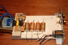
It explains the thermal drift......This is a picture of my current layout
You have pictures of good working layout in posts #54, #82 and #90. I suppose that you know why did you choose to ignore it ... 😕
looks like your jfets could still be pushed to touch each other
and the BC's ? maybe 'join' them with something heat sensitive
and the BC's ? maybe 'join' them with something heat sensitive
I started considering the layout in suggested posts. But later i wanted to try my own way only for the fun of learn a PCB design program and play around.
As i am a novice i didn't know/considered that FETs need to be thermally coupled. Thanks for help
As i am a novice i didn't know/considered that FETs need to be thermally coupled. Thanks for help
You have been a Member for 4 years.............As i am a novice i didn't know/considered that FETs need to be thermally coupled. ..........
- Home
- Amplifiers
- Pass Labs
- Preamp ideas for F5