…
I have been able to adjust the DC-offset between "IN" and "OUT" to approx. 1mV (see attached image) for both channels.
How did you do it?
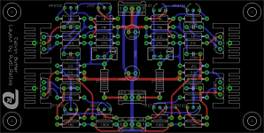
But: when I switch Power-On (I am using a standard LM317 / LM337 +/-18 VDC PSU as shown on image 2), it takes about 12-14 seconds, until the buffer finally / thermally settles.
Measuring the DC-offset after Power-On, I see it starting with a value of >1VDC (!), going down slowly to 100mV after 8-10 seconds, until it settles to about 1mV after 12-14 seconds.
I need to modify my speaker-protection circuit to support such a long-time Power-On delay.
Does anybody of you encounter this behaviour as well?
I have the impression that the time, the buffer needs to thermally settle, depends on the PSU used.
Using a simple 7818/7918 PSU gives a smaller thermal settle-time.
But I am not sure about this.
…
The 12-14 seconds it takes the output DC drift to settle down is normal, it is expected.
It is due to the master JFETs reaching operating temperature, it has nothing to do with the PSU you use.
In your PSU there is a 240 Ohm resistor in series with 10uF capacitor, which has a time constant of 0.002 seconds.
Indeed, a measure to cut off, or short, the output for about 15 seconds or more upon turning on the buffer is called for.
It can be done with a relay which has time delay, or a manual switch.
... How did you do it? ...
I do not know, Joshua!
Answer 1: the DMM is lying? But my HP 3478A is showing the same value!
Answer 2: I have done a good layout? I do not believe! Do not argue on the routing of the power tracks, please!
Answer 3: Werner has given me 2 sets of very well matched FETs! I think so!
Answer 4: I have had some luck. I think so!
Best regards - Rudi_Ratlos
Attachments
... How did you do it? ...
…
Answer 3: Werner has given me 2 sets of very well matched FETs! I think so!
…
It looks to me that this is the correct answer.

When a thread gets to 500+ posts its bound to wander. I would suggest that if any participant feels the questions are becoming repetitive or the discussion is going nowhere then perhaps its best for those involved to just withdraw and let others take up the baton of answering.
Don't make it personal. Offending posts will be removed.
Good news about PN4391.
I bought some from Futurlec: PN4391 - PN4391 N-Channel Switch Transistor .
Joshua, what brand of PN4391's are they selling?
Thanks...
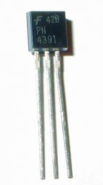
Much worse then siliconix Vishay 2N4391
I read the same think in another post somewhere on the web.
Perhaps the Siliconix devices are better in certain areas of performance?


Much worse then siliconix Vishay 2N4391
In what way are they worse and how does it established?
I read the same think in another post somewhere on the web.
…
Not everything written on the web is a factual truth, not necessarily, not always.
Please could someone check if the attached schematic have OK the G D S pin connections of JFETs?
GDS are correct, though with JFETs D and S are interchangeable.
As long as you know the gate, D and S are just arbitrary markings and are the same electrically, it doesn't matter which way around you connect it (just JFET's)
Swapping of D & S applies particularly to RF duty jFETs.
It is rarely explicitly stated that each jFET is swappable D to S.
I have tested a few k170, swapping between D&S using my LTP style jig and I find there are differences that do show in my method.
But my method is particularly sensitive to small differences in parameters.
It is rarely explicitly stated that each jFET is swappable D to S.
I have tested a few k170, swapping between D&S using my LTP style jig and I find there are differences that do show in my method.
But my method is particularly sensitive to small differences in parameters.
Swapping of D & S applies particularly to RF duty jFETs.
It is rarely explicitly stated that each jFET is swappable D to S.
I have tested a few k170, swapping between D&S using my LTP style jig and I find there are differences that do show in my method.
But my method is particularly sensitive to small differences in parameters.
What is your method and what are the differences you found?
The way JFET are constructed, there is no difference between D and S.
Another ignorant question, before to connect the buffer to the PSU LM317/337 I adjusted the PSU to give +-15VDC without load, when I connected the buffer to the PSU the voltage down to +3,91 VDC and -1,19VDC, the tx is 0-22VAC 1A main filter cap is 4.700uF
- Home
- Source & Line
- Analog Line Level
- Preamp-Buffers - simple idea