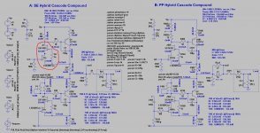
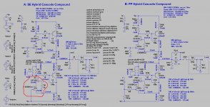
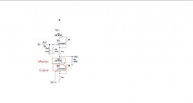
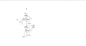
Cascode CCS master & slave in red circles of attached pic
No, J2a and J2b (which are low Vp) are masters, while J3 and J4 (which are high Vp) are slaves.
J2b and J4 are cascoded CCS, while J2a and J3 are cascoded follower.
The recommendation is to match the two masters (J2a and J2b) by IDSS and to match J3 and J4 by Vgs.
The easiest way to match Vgs is in the actual circuit. Have two matched (by IDSS) masters and instead of the slaves put some socket, so that you can swap candidate slaves, say an 8 pin socket for OpAmp. This way the circuit will operate at its' actual Id and you'll get Vgs readings which are accurate for this circuit (but only for this circuit). Don’t swap JFETs when voltage is applied to the circuit. Also, let it run for few minutes, so that the temperature will be close to the operating one.
The source resistors, R5 and R6 (which should be identical) determine the actual Id in the circuit. You don't want them to be too high, for in such a case the Vgs of the masters will be too low for linear operation. Also, you don't want them to be too high, for in such a case the Id will be too low. The Id determines the drive capability of this circuit. Between 10 to 22 Ohm seems to be a good starting point.
Ohhh Joshua thank you all is clear now. Have you news from Marko to know if the jfets that you bought to Futurlec are originals or fakes?
P.S. YHPM
P.S. YHPM
Last edited:
Ohhh Joshua thank you all is clear now. Have you news from Marko to know if the jfets that you bought to Futurlec are originals or fakes?
P.S. YHPM
No, no news from Marko, snail mail takes time…
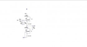
R7 & R8?
Not critical, since virtually no current flows through them. 1K will be fine.
Last edited:
Welcome Felipe,
Cin2 is probably unnecessary. Also Rin2 may be unnecessary, you can use 100 Ohm and place R4 before it.
Cin2 is probably unnecessary. Also Rin2 may be unnecessary, you can use 100 Ohm and place R4 before it.
For an lsk389 C grade, I would expect the source resistor to be lower.
2r2 is the Calvin value. I would expect the maximum value around 10r.
5mA through 10r gives a Vgs of 50mV. That may be too high, look up the datasheet graph.
Or fit a temporary 50r VR and twiddle to find an acceptable Id. Replace with a fixed value ready for testing the Cascode devices.
2r2 is the Calvin value. I would expect the maximum value around 10r.
5mA through 10r gives a Vgs of 50mV. That may be too high, look up the datasheet graph.
Or fit a temporary 50r VR and twiddle to find an acceptable Id. Replace with a fixed value ready for testing the Cascode devices.
Hi,
simulating with BobCordells LSK389C model would give ~5.4mA for 20R.
The 2R2 in the Calvin Buffer simply result from the fact that the bipolar booster current adds to the JFET current.
As the bipolar Boosters add approxiamtely 45mA the resulting current through the source resistors is 50mA, or ~9 times the current through the non-boosted cascode.
Hence the resistor needs to be roundabout 1/9th in value for the same value of voltage drop.
This voltage drop equals the Vgs of the Master JFETs.
Btw: in #441 or #442 schematics all current values are noted
jauu
Calvin
For an lsk389 C grade, I would expect the source resistor to be lower.
2r2 is the Calvin value. I would expect the maximum value around 10r.
5mA through 10r gives a Vgs of 50mV. That may be too high, look up the datasheet graph.
Or fit a temporary 50r VR and twiddle to find an acceptable Id. Replace with a fixed value ready for testing the Cascode devices.
I didn't see, attached datasheet LSK389
Attachments
no graphs/plots
look at the 2sk389 and 2sk170.
Attached 2SK389 plot/graph, wich one is & how to interpret?
Attachments
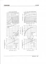
Left column, middle plot shows Vgs vs Id (=Is)
Take the highest Idss device which crosses the vertical 0Vgs axis at ~ 9.2mA
Slide down that line to the crossing @ 8mA, it reads ~-0.1mVgs
12r5 @ 8mA = -0.1Vgs
A 12r5 will degenerate a 9.2mA Idss device to ~8mA
Your currents will be quite a bit higher, so you need less resistance.
You will also be aiming for much less than 0.1Vgs, maybe around 0.05Vgs, or less.
Use the low value trimmer for your first plug board experiment to find a typical resistance at the current you want. To keep your gm high you must keep the current high. See the right column, middle plot: the 9.2mA Idss device has a gm very slightly higher than 30mS when Id = 8mA.
If you reduce the Id to 6mA the gm falls to ~27.5mS
It would be better to use a 6.1mA Idss device at 6mA, since the plot shows it has a gm of ~28mS
The closer to 100% of Idss, the better.
That is the beauty of the B1 and DCB1, they operate at 99% to 100% of Idss = maximum gm for that device.
Last edited:
- Home
- Source & Line
- Analog Line Level
- Preamp-Buffers - simple idea