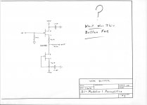
In Buf 1, (the half on the left)
the output connection is tapped into the wrong position.
The tapping should below the source resistor, i.e. at the drain of the lower jFET.
If you look at Calvin's sch you will see that the outputs are tapped in at BELOW R3 and BELOW R103.
R5 and R6 are far too low.
use >10K and preferably >100k.
Calvin uses 100k for R12 and R112.
Then use the receiver to load the cable and buffer.
You are correct.
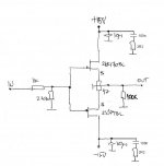
This isn't the schematic I'm going to build upon, it's only one I found on my computer with both topologies on one drawing. I meant it to serve only as an illustration of the 2 topologies I have in mind.
The topologies options I’m going to build are according to the attached schematics; one with 2 x 2SK170 (per channel) with 10 Ohm source resistors and +/- 15V supply; the other with a pair of 2SK170 / 2SJ74 (per channel) with fixed sources resistors. The 2SK170 will have a source resistor of 10 Ohm, while the 2SJ74 will have a little higher Idss and a little higher source resistor.
So, there is no need to bother commenting about the values in the attached schematics, they are given here only to demonstrate the topologies.
Attachments
Joshua, the weekend give me clear results:
1/ +-15V supply togheter 10R sounds better
2/ Changed 2SK170BL in place of LSK389, sounds better 2SK170BL
Now it's time to upgrade the PSU, I will keep you informed.
P.S. 2N4391 are on the way home to make the schematic "B" of Calvin buffer.
So using matched Idss 2SK170BL devices sounds better than LSK389?
Did you use 10R resistors for all 3 resistors, instead of 46.4R resistors?
Could a 10K volume pot be placed in front of this buffer, or would the changing impedance of the pot cause too much DC offset?
Thanks...
Hi,
I doubt about sonic differences of the parts themselves as long as its not known if everything else remained the same.
JFETs, as most any other active device, change in THD level and spectrum and sonic character depending on their working point.
These very simple circuits react due to their low psrr quite sensitive on rail line quality.
Those that Joshua shows in #401 for example react on the sheer amount of capacitance.
It seems that below ~1.000uF the bass reproduction looses on weight and authority.
jauu
Calvin
ps: a 10k Poti may safely be placed ahead of the buffers, yes
looking from the Gate of the JFET the wiper of the Poti is in parallel with the 100k resistor
The wiper impedance will vary between 0 and 2k5, paralleled with 100k.
If there were a small input offset with the 100k alone due to Gate leakage, it'd be much smaller wth the Poti in place
Last edited:
So using matched Idss 2SK170BL devices sounds better than LSK389?
Did you use 10R resistors for all 3 resistors, instead of 46.4R resistors?
Could a 10K volume pot be placed in front of this buffer, or would the changing impedance of the pot cause too much DC offset?
Thanks...
Yes, used the same pcb because I used sockets for LSK389.
Yes 10R in all places.
Why not, I use Intact Audio AVC that's an inductive autoformer volume control but you can use 10K pot.
"These very simple circuits react due to their low psrr quite sensitive on rail line quality."
Used same PSU for both JFETs.
Used same PSU for both JFETs.
Wich resistors values R5-6-7 or better how to calculate the values (I guess bias current) to make the schematic "B" using +-15V PSU?
Problems trying to match some J107s...
Using the attached circuit, I'm having trouble trying to match some J107s.
I have a momentary switch between the 10VDC source and the 100 ohm resistor Rd.
My power source is an adjustable LM317-based supply.
I'm getting varying and somewhat inconsistent results for Vab each time I measure it.
I try to take the voltage reading within a few seconds, but I don't seem to get the same reading twice.
Is there a better way to match these higher Idss devices?
Thanks...
Attachments
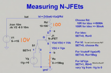
High Idss are very difficult to measure at 0Vgs
They heat up rapidly, too rapidly.
It would be better to measure them/it at the Id you intend using in the circuit.
Measure the Vgs @ operating Id.
If you are using a low gm jFET as a cascode, then even better is to use it in a cascode and measure the voltage across the lower device.
They heat up rapidly, too rapidly.
It would be better to measure them/it at the Id you intend using in the circuit.
Measure the Vgs @ operating Id.
If you are using a low gm jFET as a cascode, then even better is to use it in a cascode and measure the voltage across the lower device.
Measure the Vgs @ operating Id.
What's the operating Id point for schematic B, C and D?
High Idss are very difficult to measure at 0Vgs
They heat up rapidly, too rapidly.
It would be better to measure them/it at the Id you intend using in the circuit.
Measure the Vgs @ operating Id.
If you are using a low gm jFET as a cascode, then even better is to use it in a cascode and measure the voltage across the lower device.
The other device is the PF5102, which I assume are supposed to be matched for the Calvin buffer, as well.
Can you please draw a circuit, or post a link to a comparable circuit, showing what you mean by "to use it in a cascode and measure the the voltage across the lower device" as I have no idea what you're suggesting?
Thanks...
which post are sch B, C and D shown in?What's the operating Id point for schematic B, C and D?
The cascodes are shown in post397for the Calvin buffer, as well.
Can you please draw a circuit,
j2/j1a are a cascode pair as are j3/j1b & j102/j101a & j103/j101b
Taking the top left as an example:
J2 has the full voltage applied to it. It is the cascode device.
Since no gate current flows the voltage at both ends of R4 are the same, i.e. J2 gate is at the same voltage as J1a source.
J1a has a Vds that J2 source voltage - J2gate voltage = Vgs of J2
The current through J1a is Id and it is the Id when Vgs =0 and Vds = it applied voltage. The applied voltage is J2 Vgs.
You set up a plug board with J2 and J1a wired as the sch connect J1a gate to J1a Source Connect R4 add in R2 = 180r to replicate the sch.
Apply a voltage of Vp across the assembly. try 10v and then measure the the Vds of J1a. Measure Vgs of J2 these two measurements should be the same. Now increase Vp to the full 15V and remeasure. You can now measure the Vdrop of R2 and from that calculate Id.
You now have the Id of J1a when Vds is your measurement.
You also have the Vgs and Vds of J2 when Id is passing.
Different devices for J2 will give slightly different Vds and Vgs
Select some pairs of J2 that give similar measurements.
Now keep one of those J2 in place and this time sway in different J1a.
again from all the devices select some that make close pairs.
Use the selected pairs as the j1a/b and as J2/3
This matches up the two sets of cascodes to operate at nearly equal voltages and nearly equal currents. This gets best performance from the upper and lower cascodes.
If you have stereo, try to find match quads for each device and then split the quads so that left and right use best pair that match channel to channel.
If you put
which post are sch B, C and D shown in?
Post 1.
Attachments

You set up a plug board with J2 and J1a wired as the sch connect J1a gate to J1a Source Connect R4 add in R2 = 180r to replicate the sch.
Apply a voltage of Vp across the assembly. try 10v and then measure the the Vds of J1a. Measure Vgs of J2 these two measurements should be the same.
Andrew, thank you!
OK, posted is the circuit I will be building on the left and what I think is the circuit you suggested building for matching devices on the right.
Is the circuit on the right all I need, or do I need to include more of the original circuit?
I will just use a 180 ohm resistor in place of the 100 and 75 ohm resistors.
Where do I connect the ground from the power supply? I only see a ground connection at the bottom of R115.
Attachments

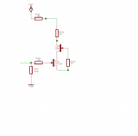
take out R116 and R115.
connect the Q19 Gate to Q19 Source, i.e. place both leads into the same rail of the plug board.
Take out R101
Replace R102 with 180r, to match the Calvin Buffer.
You have two resistors and two jFETs in the testing jig.
You have ONE power supply: 0V and +15V
Connect 0V to the G+S of Q19. Bottom of R104 also goes to here.
Connect +15V to top of R102.
Forget the word "ground" it causes confusion all over this Forum.
which post are sch B, C and D shown in?
using sch BPost 1.
the Id of the lower device (J2b) is also the Id of the upper device (J4), since the gates do not pass DC current, until you overload them.
The lower device has a source resistor (R6).
The value of that source resistor has a profound effect on the current that flows from the source.
You can measure your device Idss and use the plots in the datasheet to estimate the Id that would flow for any particular device and resistor value.
It is far easier to just measure the Id with the actual device and the actual resistor. Use a plug board.
The cascode/upper device (J4) needs to apply sufficient voltage (Vds) to the lower device to get proper operation. Borbely tells us that the Vds of the lower device should be at least 2times Vp of the lower device. This 2times Vp rule also applies to the upper/cascode device. But the cascode device has a MUCH higher Vp and thus NEEDS a much higher Vds to operate properly.
Measure Vp and Idss of BOTH devices using the Borbely test jig.
Last edited:
You now have the Id of J1a when Vds is your measurement.
You also have the Vgs and Vds of J2 when Id is passing.
Different devices for J2 will give slightly different Vds and Vgs
Select some pairs of J2 that give similar measurements.
Now keep one of those J2 in place and this time sway in different J1a.
again from all the devices select some that make close pairs.
Use the selected pairs as the j1a/b and as J2/3
This matches up the two sets of cascodes to operate at nearly equal voltages and nearly equal currents. This gets best performance from the upper and lower cascodes.
If you have stereo, try to find match quads for each device and then split the quads so that left and right use best pair that match channel to channel.
I built the test jig and got it working.
Using a 15V supply, I measured a Id of 8.8mA(1.54Vdrop across 175 ohm resistor) for J1a(PF5102).
You're correct about Vds of the PF5102 being the same as Vgs of the J107.
Leaving a PF5102 in the circuit and swapping in different J107s I got a pretty large voltage spread from 2.08V-2.79V.
I was able to find 2(sometimes 3 devices) that had exactly the same voltage reading, which I set aside as a matched pair or trio.
For example I found 2 that both measure 2.60V, 2 that both measure 2.21V, etc..
Leaving one of the matched J107s in the circuit, and swapping in different PF5102s, the voltage spread is less from 2.14V-2.28V. These seem to be easier to match up because they measure closer to one another than the J107s do.
So, are we matching devices here by voltage instead of Idss?
Thank you...
Hi,
basically Id or Vgs are the two sides of the same coin.
For this application though shall the Master JFETs be matched for same Id and optionally the cascoding Slaves for same Vgs.
- Current for the Masters as their drain current generates a voltage drop over R101/102 and R108.
The Slave's drain current equals the Masters drain current, so it doesn't influnce here.
This voltage drop then opens up the bipolar Boosters and defines the current trough them.
As the Booster current contributes much more to the combined current through R106 and R111, we want the JFET and Booster currents to be equal.
- Voltage for the Slaves as their Gate-Source voltage equals the Drain-Source voltage of the Masters, the parameter we want to be equal in upper and lower branch.
The drain current of the Masters depends slightly in their drain-source voltage.
But since the variations of Id over Vds are comparably small, the variations in the Slave's Gate-Source voltage doesn't count as much.
Iow: Id matching of the Masters is the prime goal.
Voltage matching of the Slaves just puts the . on the i.
jauu
Calvin
The cascode/upper device (J4) needs to apply sufficient voltage (Vds) to the lower device to get proper operation. Borbely tells us that the Vds of the lower device should be at least 2times Vp of the lower device.
Do you refer to J2b?
- Home
- Source & Line
- Analog Line Level
- Preamp-Buffers - simple idea