Both the upper device and the lower device should have at least 2times Vp applied as a Vds.
If the devices are different then the Vp can be different.
That results in the minimum Vds for each device being different.
You should be looking at EACH device individually.
Go and read Borbely.
If the devices are different then the Vp can be different.
That results in the minimum Vds for each device being different.
You should be looking at EACH device individually.
Go and read Borbely.
Thanks Andrew, Erno uses current limiting diodes 2mA and 5mA, wich one have I to use? could I use +-12V in place +-10V for Borbely jig?
Last edited:
The jFET with gate connected to source is a CCS. You don't need another CCS.
The resistor in the source lead changes the Id of the jFET, i.e. the resistor sets the CCS current value.
The outer/upper jFET cascodes the CCS. This cascode isolates the CCS from voltage changes and also from excessive voltage.
The outer device is not a CCS. It is a voltage controller. It controls the voltage fed to the CCS.
You need to read Borbely again and if need be ten times.
I explain't very bad as usual, my question was related to Borbely jig to measure jfets & I know what's the purpose in his jig of current limiting diodes, the question is: what current limiting diodes have I to use to measure Vp for Calvin buffer schematic B?
Last edited:
measuring Vp does NOT need a current limiting diode.
Vp requires a dual polarity voltage/current supply, a 1M0 or slightly higher resistor, a voltmeter.
The 1M0 resistor sets the Id to ~10uA since there is ~-10V across 1M0.
The voltmeter measures the voltage from Gate to Source, i.e. Vgs when the Id is ~10uA
You need to read Borbely again and again until you understand enough to ask the right questions about the bits you don't understand.
A k170 in the BL grade will have a Vp ~500mVdc to 1Vdc
GR grade quite a bit less, maybe around 300mVdc to 600mVdc
A low gm device with the same Idss will be very much higher Vp.
8mA Idss k246 might be Vp from 2Vdc to 3Vdc
A 20mA low gm jFET could have a Vp approaching 5Vdc.
i.e. it needs a Vgs of close to -5V to almost switch it off.
GR grade quite a bit less, maybe around 300mVdc to 600mVdc
A low gm device with the same Idss will be very much higher Vp.
8mA Idss k246 might be Vp from 2Vdc to 3Vdc
A 20mA low gm jFET could have a Vp approaching 5Vdc.
i.e. it needs a Vgs of close to -5V to almost switch it off.
Thanks Andrew for your patient, Erno wrote:
"The next two positions measure the VGS for the device at given drain currents.
These positions give practical readings for design purposes, and you can choose the constant-current sources for the values you need."
If I don't know the given drain current how can I choose the constant-current sources necessary values for the circuit?
You don't need them to assemble the cascodes.
You can select high gm devices by Idss (use the Borbely jig)
The high Idss devices used in the cascode will usually not allow accurate Idss to be measured, because the junction temperature rises too quickly and eventually too far and you blow up the jFET.
Instead, assemble the cascode arrangement as your measuring jig and measure the upper device Vgs as your matching criteria. The actual Id depends on the lower device gm and source resistor value. But you don't need to know that. You can measure it using the Vdrop of the 180r resistor, but you don't actually need it.
Using an Idss for the lower device and a Vgs as applied by the upper device gets you to a very close matching of the 4 devices in a Calvin Buffer.
Will be more usefull if Calvin posted in the schematic the Idss values of JFETs and the resistors values.
Last edited:
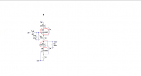
NoAre these red marked the lower devices?
Do you know what a jFET wired as a CCS looks like?
Do you know what a cascode added to a jFET looks like?
Before you delve into these projects you need to have some background understanding.
Read Borbely, then formulate your questions.
as I posted earlier
Which part of that don't you understand. ASK !The cascodes are shown in post397
j2/j1a are a cascode pair as are j3/j1b & j102/j101a & j103/j101b
Do you understand that?J2 has the full voltage applied to it. It is the cascode device.
Last edited:
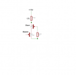
JFET wired as a CCS looks like
Cascode added to a jFET looks like
An externally hosted image should be here but it was not working when we last tested it.
Cascode added to a jFET looks like
No.
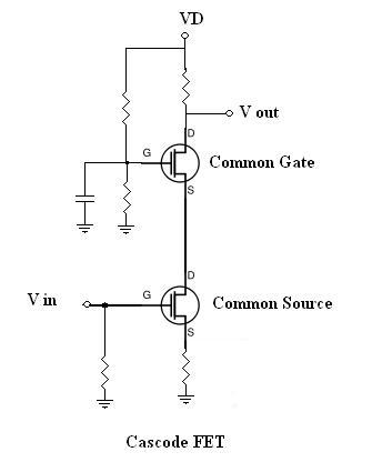
In the upper/first diagram:
Q1 is the CCS.
RV1 sets the CCS current.
Q2 is the cascode. It is wrapped around Q1.
The pair are a cascoded CCS.
If you refer to the datasheets of the j113 and the 2sk209 you will find the gm of these devices. You may also find the Vgs vs Id plots in there as well.
I would expect the gm j113 < gm 2sk209
I would expect the slope of the Vgs vs Id curves to be different as well.
One chooses a High Vp device as the cascode and chooses the Low Vp device as the CCS. This is to ensure they meet the Borbely 2 times Vp rule.
The second diagram does not has a CCS, nor does it have a Cascode.
However, the common gate circuit does set a near constant voltage at the drain of the common source amplifier. It has a cascoding effect.
You really do need more knowledge, to get into this hobby.
Last edited:
That device needs a Vds of > 0.88V
When the 2r2 source resistor is added, the Id will be < 6.6mA, maybe around 5mA
When the 2r2 source resistor is added, the Id will be < 6.6mA, maybe around 5mA
Yes, cascoded CCS in the lower halves. Cascoded follower in the upper halves.
That sch is different.
It does not have the 2r2 source resistors setting the CCS current.
That sch is different.
It does not have the 2r2 source resistors setting the CCS current.
Last edited:
Hi,
basically Id or Vgs are the two sides of the same coin.
For this application though shall the Master JFETs be matched for same Id and optionally the cascoding Slaves for same Vgs.
Iow: Id matching of the Masters is the prime goal.
Voltage matching of the Slaves just puts the . on the i.
Boy...I'm still a little confused here.

I'm using the simple circuit Andrew suggested below.
Are you saying it's better to match the Master devices by measuring the voltage drop across the 175 ohm resistor for Id, or can I just measure their Vds(using the same Slave device) and match them like Andrew suggested?
Like with a lot of things I do, I'm probably making this more complicated than it needs to be.😱
Attachments
Hi,
proceed as Andrew suggested.
Then You will have two matched Masters and two matched Slaves.
Measuring the voltage drop over over their common drain resistor (175R) is then just a final control.
If You only match the Master-Slave pairs for same voltage drop over the 175R, then the following could happen:
- say, the Masters differ in Idss and the Slaves differ in Vgs
- a combination of the first Master having a slightly higher Idss with a first Slave having slightly less Vgs, and the second Master with lower Idss beeing cascoded with a second Slave with more Vgs (mean value, neglecting the minus sign in Vgs).
- both combinations may lead to equal Id values through and equal voltage drops across their drain resistors, but may be slightly misatched 'internally'.
Varying the source resistor of the Master has a much greater effect on the Id than varying its drain-source voltage (which is at the same the Slave's gate-source voltage).
So, if one measures equal voltage drops over the common 175R drain resistors this would mean a sufficient close Id matching of the Masters and Vgs matching of the Slaves for this Application.
If your application requires more precision You need to match Masters and Slaves separately.
This could be the case if You want to optimize THD and/or temperature behaviour.
Temperature is the third parameter that affects the Id.
It creates an offset voltage at he output of the circuit.
Again the Master's behaviour is dominant in all shown circuits of this thread.
Matching the Masters should therefore be done under similar temperature conditions.
Sounds easier as it is, as especially measuring the Idss means high heat power losses and conditions close to thermal destruction.
The high Idss (~100mA) of the Slaves heats them up fast and generates heat power that the device can't take for long.
No wonder that You get inconsistant results, because You can at most only measure whilst the warming up phase of the device, as the thermal equilibrum would be beyond the thermal limits.
So, for the high Idss high Vgs Slaves matching should only take place around the specified Id of the circuit.
The two Masters can be -and maybe shall be- thermally coupled (a advantage of the Dual LSK389 over single devices).
The Calvin Buffer seems to reach thermal stability wo. thermal coupling of devices as the Hesener variant prooves, but don't take that for granted under all circumstances.
Thermal coupling of the two Masters is helpful in any case.
Inclusion of the cascoding Slaves is optional.
The bipolar boosters must not be thermally coupled to the Masters or the cascodes!
They require their own separate heatsinks.
jauu
Calvin
- Home
- Source & Line
- Analog Line Level
- Preamp-Buffers - simple idea