Hi,
read the thread. It's been written a couple of times which non-obsolete devices in which casings are suitable.
It seems that generally JFETs fabricated after process 51 will work here.
jauu
Calvin
read the thread. It's been written a couple of times which non-obsolete devices in which casings are suitable.
It seems that generally JFETs fabricated after process 51 will work here.
jauu
Calvin
@AMMEL68:
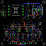
The Calvin-Buffer-PCBs that I am offering use R1206 - SMD - resistors.
I have done a new layout for Calvin's buffer especially for you, using "standard through-hole resistors".
The layout does even include a LM3x7 based PSU for the buffer.
It uses a TAMURA 3FD-436 transformer rated a 2x18VAC / 170mA per secondary winding, and I will adjust the layout to both support 230VAC and 115VAC mains.
I wonder, if Calvin has some objectives against including a PSU on his buffer PCB.
So long I have never had any troubles (hum) using a TAMURA-transformer / PSU.
But if Calvin tells: "Do never do this ..." - forget about this layout.
If he does not: I will happliy send you the Gerber files to etch this PCB by your own.
Best regards - Rudi_Ratlos
P.S.: The PCB-size is 100 x 100mm.
Attachments
Though the circuit is simple enough to build on a perforated board, if anyone has Through-Hole PCBs, I'm interested.
Hi Rudi,
Thank you.
On a second thought, I'd rather use perforated board, since I want the 4 JFETs on each channel mounted with EUVAL's mini-heatsinks.
Also, I have no intention to have the PSU in the same case with the buffer and I intend using Jung's Super regulatpr.
Thank you.
On a second thought, I'd rather use perforated board, since I want the 4 JFETs on each channel mounted with EUVAL's mini-heatsinks.
Also, I have no intention to have the PSU in the same case with the buffer and I intend using Jung's Super regulatpr.
Hi,
read the thread. It's been written a couple of times which non-obsolete devices in which casings are suitable.
It seems that generally JFETs fabricated after process 51 will work here.
jauu
Calvin
Hi Calvin,
After glancing through most of the posts here, since I don't have the time to read every post in detail, I saw quite a few devices listed.
2SK369/J310...FZT751/53...BF862/SST4391 and BC847BS.
I don't know what process 51 is.😕
Getting back to my original question, what are the preferred input devices for your buffer?
Thanks...
Hi,
Rudi, of course don´t I object if You doe Your own layout with ower supply included.
It´s simply not my business 😉
If something doesn´t function as supposed I´ll say: "It´s not my fault. It was broken already" 😀
Just a few words regarding Your layout:
It leaves room for improvement.
The routing of the gnd and supply lines is off of optimal.
As a design tip for power supplies start with routing a thick gnd ´beam´ and the two supply voltages on the other copper layer. The gnd covering the supply lines, like this
__ __ top layer, pos, neg.
XXXXX PCB core layer, FR4
_____ bottom layer, gnd
The probability of long inductive loops is mimimized and the sandwiched layers form a distributed capacitance.
Then place the parts around this ´centre beam´.
It´ll most certainly look totally different to Your schematic layout and not as logical either, but it will be better signal-wise.
The two Master JFETs could be thermally coupled, but not on the same cooling fin as the bipolar Slaves.
You may of course apply the same layout technique not only to the power supply part but also to the signal part of the PCB, or when using direct wiring on a perforated board.
Ammel:
The PF5102/J107 have proven good, as well as 2SK170/4391, BF862/4391 and 4393/4391.
Process 51 is a manufacturing process.
One can divide all JFETs into groups, like low-noise, high input impedance, HF, switching, high gm etc. etc.
Lownoise for example requires large Gate geometries, which increases Capacitance, HF requires the opposite low capacitance.
So two differing geometries of the layout on the die are required.
JFETs produced after a certain common process share distinct properties.
It´s similar to automobiles. SUVs form a family within the species car.
And this family differs from the Van family of cars or the Coupe family.
jauu
Calvin
Ammel:
The PF5102/J107 have proven good, as well as 2SK170/4391, BF862/4391 and 4393/4391.
Hi Calvin,
I'm having trouble finding these devices since it looks as though most are obsolete.
The PF5102 is currently available, but the J107 is a no-go.
I have some 2SK170's, but the 4391 looks like another no-go.
So, can this buffer be built with any available FET's, or do you know of a source for them?
Google is your friend, at Mouser you can find J107: J107 Fairchild Semiconductor | Mouser and at Futurlec you can find PN4391: PN4391 - PN4391 N-Channel Switch Transistor .
Hi,
the SK170 are available as LSK170 from Linear Sytems.
Linear also produces the LSK389, the Dual LSK170
IIrc there's another new JFET from LSK, the LSK845, that should do well too.
The 4391 are produced by several manufacturers with different suffixes and in different casings.
PN stands for TO-18 metal can, manufactured for example by Interfet.
Btw: Interfet is specialised on JFETs, producing a row of otherwise obsolete parts.
Their process numbers differ from those of National Semi.
IIrc the intersting process numbers are 16 and 132 (low noise and switching JFETs).
Search their website for a pdf about their process numbers.
2N is the plastic TO-92 casing.
SST was used by Fairchild and iIrc Vishay, both now obsolete (SOT23).
MMBF is used by OnSemi for their SOT23.
PMBF is another SOT23, I assume made by NXP/Philips.
jauu
Calvin
Beware of fakes from Futurlec.
2SK170/J111 and BF862/MMBF4391 are good combinations & easy to find.
2SK170/J111 and BF862/MMBF4391 are good combinations & easy to find.
Hi,
Thank you.
Do you know that they have fakes at times, or is it just a general suspicion?
I already ordered some PN4391 from them, how can I tell if they are genuine or fake?
Beware of fakes from Futurlec.
…
Thank you.
Do you know that they have fakes at times, or is it just a general suspicion?
I already ordered some PN4391 from them, how can I tell if they are genuine or fake?
Me got fakes in the past, but they were 2SK117 & 2SK170.
To be 100% sure, you should check PN4391 with curvetracer.
If you don't have one or don't know anyone with curvetracer, you can send 1 pcs to me. I can compare PN4391 with my MMBF4391.
To be 100% sure, you should check PN4391 with curvetracer.
If you don't have one or don't know anyone with curvetracer, you can send 1 pcs to me. I can compare PN4391 with my MMBF4391.
Me got fakes in the past, but they were 2SK117 & 2SK170.
To be 100% sure, you should check PN4391 with curvetracer.
If you don't have one or don't know anyone with curvetracer, you can send 1 pcs to me. I can compare PN4391 with my MMBF4391.
Hi,
Thank you very much.
Neither me nor anyone I know of in my country have curve tracer.
Once they'll arrive, I'll send you one. I'll PM you about it.
If they are fake, I'll order some J111 from Mouser.
Hmm... Interesting ideas floating around. The only discrete followers I've seen in HiFi equipment were CFP BJTs with a resistor making up the other half. In the long term it's easier to use an op amp of course but where's the fun in that?
Google is your friend, at Mouser you can find J107: J107 Fairchild Semiconductor | Mouser and at Futurlec you can find PN4391: PN4391 - PN4391 N-Channel Switch Transistor .
Thanks Joshua...I always use Google, but I was adding a 2S prefix in front of the J107. No wonder nothing turned up.😱
Hi,
the SK170 are available as LSK170 from Linear Sytems.
Linear also produces the LSK389, the Dual LSK170
IIrc there's another new JFET from LSK, the LSK845, that should do well too.
The 4391 are produced by several manufacturers with different suffixes and in different casings.
PN stands for TO-18 metal can, manufactured for example by Interfet.
Btw: Interfet is specialised on JFETs, producing a row of otherwise obsolete parts.
Their process numbers differ from those of National Semi.
IIrc the intersting process numbers are 16 and 132 (low noise and switching JFETs).
Search their website for a pdf about their process numbers.
2N is the plastic TO-92 casing.
SST was used by Fairchild and iIrc Vishay, both now obsolete (SOT23).
MMBF is used by OnSemi for their SOT23.
PMBF is another SOT23, I assume made by NXP/Philips.
jauu
Calvin
Thank you for the explanation, Calvin.
As I noted above, I was searching for a 2SJ107 instead of just J107.😱
All of the 2N4391's I've found have been in a metal can TO-18 package, instead of TO-92. Looks like the PN prefix is for TO-92.
They're quite expensive too at around $2 USD each. Certainly not a device I could buy many of for matching purposes, unless you're rich.
Hi,
with the Cordell model LSK389CCo following results simmed for Zout of circuit´A´.
R2/3: 1,0 mOhm -> Id: 8.64mA -> Zout: 34.7Ohms
R2/3: 4.7 Ohm -> Id: 7.63mA -> Zout: 41.1Ohms
R2/3: 10 Ohm -> Id: 6.78mA -> Zout: 48.2Ohms
R2/3: 22 Ohm -> Id: 5.47mA -> Zout: 63.8Ohms
jauu
Calvin
Hi,
I have two LSK389 are 8 mA, could I use jumper for R2/3?
TIA
Felipe
- Home
- Source & Line
- Analog Line Level
- Preamp-Buffers - simple idea