I'm very interested in your state: "only 1 Pair Mosfets required for High Power 500 - 1000W".
Could You share Gerber and schematic?
This working only with Class TD (Tracking Down Rail switcher)
effiiciency similar like class D, but its Analog Class AB NMOS amp
without big heatsinks.
To drive 4 IRFP240 buffer will be good, because driving capacitive load
look sample schematic from Power Mosfet Amp
Attachments
Last edited:
Discrete Front End V/S OP amp input stage is asking for trouble, you need matching low noise Transistor, DUAL low noise Transistor pair obsolet and much more components without any benefit.
If you have counterfaits fake discrete Transisitor in Front End, NMOS amp have audible hiss.
I have starting 10 years before with Original NMOS, but have change very much
OP AMP NE5534A or LM318 Front End, DC Protect Triac Crow Bar,
Display Anzeige with Clip Limiter, Cascoded VAS
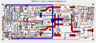
If somebody like it can share Gerber
Class TD extension PCB not finished and tested
If you have counterfaits fake discrete Transisitor in Front End, NMOS amp have audible hiss.
I have starting 10 years before with Original NMOS, but have change very much
OP AMP NE5534A or LM318 Front End, DC Protect Triac Crow Bar,
Display Anzeige with Clip Limiter, Cascoded VAS
If somebody like it can share Gerber
Class TD extension PCB not finished and tested
Attachments
Welcome back Quasi!!!
Great amps, I built 4 of them within last several years.
Thanks! Hope they all still work!
Cheers
Q
Welcome back Quasi. Still enjoying the NMOS200.
Thanks Givingitago. I think the Nmos200 is the most popular version. A while ago I even saw the the PCB for sale on Ebay.
Cheers
Q
Hello Quasi,
nice to see you come back
I think to add external 12V for symmetrical Clipping could be good idea?
To avoid Mosfet oscillation Ferrit Bead or resistor and condensator in series Gate do Drain should be look PIC
Thanks Malta, and thanks for the suggestions.
Cheers
Q
Hi Quasi,
I have build 10 years ago your NMOS
NMOS MK3 should have real impovements
1 pcs. Mosfet FDA69N25 can replace 3 -4 pcs. IRFP240, save cost and space
To improve efficiency from NMOS we should add CLass TD Rail switcher its
cheap with less components, dissipation for NMOS about 50W at fullpower compare before about 400W
1 pcs. Mosfet FDA69N25 is more enough for full output power
look attachment schematic tracking Downconverter
Are any Nmos still working. Are you happy to share your schematics?
Cheers
Q
Greetings - long time no Quasi.
Anyway started playing around again, trying to improve the Nmos350 / 500. A few changes around the second stage, component values throughout and tiny bits of filtering to add more control.
This is the SIM, not perfect but not bad. Looking forward to further improving it with your ideas. SIM file plus screen shots to follow.
Can you upload an asc sim that can be run, with settings and all.
As it is not it can't.
Can you upload an asc sim that can be run, with settings and all.
As it is not it can't.
I'm not sure how to do that. Do you have LTSpice installed? Or what else do I need to upload?
Cheers
Q
Yes working, but original NMOS had very small hiss, barely audibleAre any Nmos still working. Are you happy to share your schematics?
Cheers
Q
Yes will share
Hello NMOS,I forget
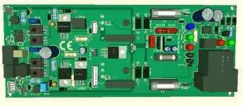
LED Status
ON Power
Signal
Clip
Clip Limiter
contact me if interested, I share Gerber and schematic
If you are using IXYS: IXTK46N50L / IXTK110N20L2
only 1 Pair Mosfets required for High Power 500 - 1000W
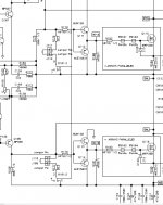
PCB Quasi ACTRK 600 amp is small 160 x 80 mm
IXYS: IXTK46N50L / IXTK110N20L2
some years ago I proposed an output stage with the IXIS L2 MOS devices, but there was no much interest.
Vertical MOSFETs for a PA amplifier OP
Could you share some more details on you experience with them?
Did you actually build? I am am particularly interested in how to get rid of all that power dissipation with a single device.
Thanks
Hello NMOS,
some years ago I proposed an output stage with the IXIS L2 MOS devices, but there was no much interest.
Vertical MOSFETs for a PA amplifier OP
Could you share some more details on you experience with them?
Did you actually build? I am am particularly interested in how to get rid of all that power dissipation with a single device.
Thanks
" I am am particularly interested in how to get rid of all that power dissipation with a single device"
Class EEEngine rail tracking do the job with very low power dissipation
Class AB Amplifier can be efficient same like Class D.
The KEY is Rail tracking, in this case 1000W Class AB Amplifier have 100W Dissipation.
Class EEEngine / Class TD rail tracking do the job
For example 3 pair MJL3281 can deliver 2500W 4 Ohm
Rail 140-150 V DC
Are any Nmos still working. Are you happy to share your schematics?
Cheers
Q
Hello Quasi
are you interested to upgrade ACTRK 400/600 with High efficiency Rail Tracking ?
Hi NMOS,
Now you're talking about a Carver Lightstar. Each channel has its own down converter?
By the way, this was very effective at keeping the heat down while also being very reliable.
-Chris
Now you're talking about a Carver Lightstar. Each channel has its own down converter?
By the way, this was very effective at keeping the heat down while also being very reliable.
-Chris
Yes I would NMOS. I presume it would be a switching supply otherwise there would be little point I guess.
Hi Chris, long time no talk.
Hi Chris, long time no talk.
Last edited:
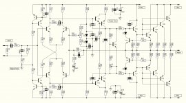
Hi folks,
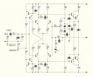
A little out place here but I wanted to ask a question about an amp cct I'm tinkering with. It concerns the thermal and current stability of the 2nd stage.
This is what I'm worried about. Excluding T9 & T10 for the moment, Transistors T11 & T12 are driven by the voltage across R11 & R33 and this sets the current through them. What happens to the current when T11 & T12 get hot (and they will). I'm worried that a current increase here will make a big difference to the idle current of the output stage (not shown).
Attachments
Yes I would NMOS. I presume it would be a switching supply otherwise there would be little point I guess.
The amp will have 1 fixed Rail 60 - 140 V DC
1 - 2 pair 500W Mosfets enough up to 90 V DC
Tracking Buck Converter gives Class D Efficiency,
140 V DC - 2 to 3 pair 500W Mosfets enough
With BJTs MJL3281C you need 3 pair for 140V DC Rail
Output Impedance 2-8 Ohm
With BJTs amp is working without issues, lets try with ACTRK soon
Last edited:
Hi quasi,
Always a pleasure! Yes, too long.
Thermally bond T9 to T11, T10 to T12. You can't forget about T9 and T10 as they will affect the bias. I don't use spice, but at this point I would build it up and try it even if I did.
What are your rails and transistor types? This could be a signal amp or scale up to a medium powered amplifier.
Best, Chris
Thanks Chris,
This is the full schematic of what I had in mind. Split rails to achieve rail to rail output - it Sim's to less than 1v of rail. I started designing the PCB when I became worried about the thermal problem of the second stage.
Transistors:
CCS: BC546 & BC556
Input stage - 2SC1845 & 2SA992
Second stage - not sure yet
Driver & Output stages NJW0281G & NJW0302G
Sadly not a Quasi, although it could be.
Cheers
Attachments
Last edited:
- Home
- Amplifiers
- Solid State
- Power amp under development