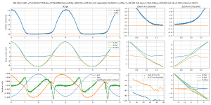
Hyperbolic diodes:
This is "non-switching" so how does it handle the turn-off spike test?
It turns out pretty terrible. BJTs without resistors and low impedance CFP drivers gave a much better result earlier in the thread.
This is "non-switching" so how does it handle the turn-off spike test?
It turns out pretty terrible. BJTs without resistors and low impedance CFP drivers gave a much better result earlier in the thread.
Attachments
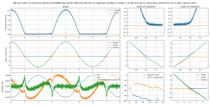
Hyperbolic diodes with constant bias:
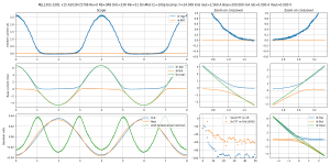
No spikes at all, even on hard mode, at 48kHz 2.56A! This is an excellent result ; unfortunately this circuit makes a lot more static distortion than the plain resistor-free BJT, so it still loses.
Both this one and the previous post use the same Schottky diodes, and output current is high enough to make them turn off. The previous measurement has spikes, this one does not, which means that Schottky diodes do have the expected soft clean turn-off.
Therefore, the mess comes from the bias circuit that imposes a constant voltage across the diodes. As shown previously, if the transistors turn off, the feedback loop is broken, and the bias circuit just loses it. I added a resistor to prevent them from turning off, but my guess is that the Schottky diodes capacitance is high enough to steal all the current from this resistor, which causes emitter current to reach zero anyway, which turns off the transistor.
That means this circuit won't work.
Attachments
-
 scope-Bias=200.000 mA Iout=2.560 A F=48.000 kHz--MJL1302-3281 v15 A2039-C5706 Re=STPS40M60 Ree=6.png269.1 KB · Views: 272
 -
 scope-Bias=200.000 mA Iout=2.560 A F=24.000 kHz--MJL1302-3281 v15 A2039-C5706 Re=STPS40M60 Ree=6.png259.8 KB · Views: 270
 -
 scope-Bias=100.000 mA Iout=2.560 A F=48.000 kHz--MJL1302-3281 v15 A2039-C5706 Re=STPS40M60 Ree=6.png259.1 KB · Views: 272
Amazing work!
It would however make it easier for me that don't follow all the terminology if you could post a schematic of the tested circuit together with the measurements. Please do it for the dummies? 🙂
It would however make it easier for me that don't follow all the terminology if you could post a schematic of the tested circuit together with the measurements. Please do it for the dummies? 🙂
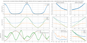
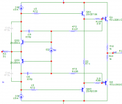
Back to basics, then.
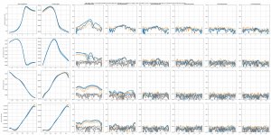
I tested this schematic before, and found it to be a bit unstable without the 100pF compensation capacitors. With the compensation caps however, it seems to work just fine.
I didn't install the fiddly temperature probe, so this is not thermally compensated at all. So, under load, actual bias is about 20-30% more than what it says on the graph.
Turn-off behavior is pretty much identical to the circuit with the CFP drivers... but without the temperamental CFP drivers, which is excellent. Current gain is much lower of course, because the CFP drivers have two driver hFes, and this one has just one driver hFe. A good spot to add a predriver would be to turn the two input transistors into Rush "cascodes".
This is the current leader.
Attachments
-
 resistor free sense driver emitter.PNG31.9 KB · Views: 281
 -
 scope-Bias=200.000 mA Iout=2.560 A F=48.000 kHz--MJL1302-3281 v15 A2039-C5706 Re=0 Rb=3R8 DrE=33.png269.5 KB · Views: 190
 -
 scope-Bias=100.000 mA Iout=2.560 A F=48.000 kHz--MJL1302-3281 v15 A2039-C5706 Re=0 Rb=3R8 DrE=33.png266.7 KB · Views: 186
Amazing work!
It would however make it easier for me that don't follow all the terminology if you could post a schematic of the tested circuit together with the measurements. Please do it for the dummies? 🙂
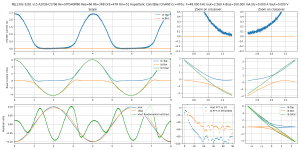
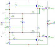
I put the "hyperbolic" schematics next to the name in bold in the previous page, but yeah, I felt the same, so I put schematics in the prev post 😀
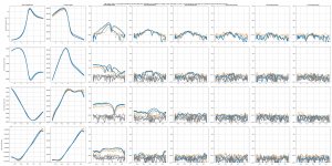
In the previous circuit, the bias control transistors regulate the voltage between driver emitters, keeping it constant.
If I simply move the point where they sample their input voltage to the OPT bases instead... that's moving the wires coming from the right side of the two 470R resistors from the driver emitters to the OPT bases... then it will keep the voltage between power transistor bases constant instead, and compensate the voltage drop on their base resistors.
Due to OPT base current, there is voltage drop across the base resistors, which reduces the bias voltage between OPT bases when under load, which means it will behave under load as if it had less bias. By removing this effect, this mod basically adds "free" bias current.
It should also remove some of the distortion introduced by hFe mismatch creating voltage drop on the base resistors.
The effect is small, but it is not zero, and the mod is free, so why not.
Attachments

Looks good! 🙂
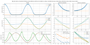
Excuse me for littering the thread with stupid questions.. Both the measurements in the last posts are with the sensing points moved to output bases I assume. What is the parameter changed between the two? The right one looks smoother and more symmetrical. Iq noted to be 200mA in both cases? Or is it actually 100 and 200mA as the previous one? Looks like the error voltage is smooth, so it should not have a lot of higher harmonics.
Excuse me for littering the thread with stupid questions.. Both the measurements in the last posts are with the sensing points moved to output bases I assume. What is the parameter changed between the two? The right one looks smoother and more symmetrical. Iq noted to be 200mA in both cases? Or is it actually 100 and 200mA as the previous one? Looks like the error voltage is smooth, so it should not have a lot of higher harmonics.
No worries 😀
In post 424, bias control transistors measure voltage between driver emitters
In post 426, between output transistor bases
> The right one looks smoother and more symmetrical. Iq noted to be 200mA in both cases?
Yeah, because the difference is frequency (48k vs 24k), I attached the wrong plot lol. It's written in the figure title but that's a mess.
--
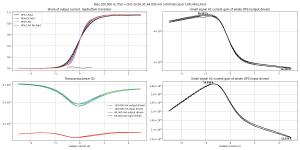
Now, the distortion test for both circuits above!
This is for the schematic in post 424, bias control transistors measure voltage between driver emitters.
Title says 100mA bias, but since the thermal compensation circuit with temperature probes on transistor collectors is not installed, it looks like it used about 30% more current (watching the power supply indicators right when the signal stops)...
There's not much distortion, and the 3rd harmonic due to Early effect/input capacitance is also gone, cleaned up by feedback from the bias control transistors.
In post 424, bias control transistors measure voltage between driver emitters
In post 426, between output transistor bases
> The right one looks smoother and more symmetrical. Iq noted to be 200mA in both cases?
Yeah, because the difference is frequency (48k vs 24k), I attached the wrong plot lol. It's written in the figure title but that's a mess.
--
Now, the distortion test for both circuits above!
This is for the schematic in post 424, bias control transistors measure voltage between driver emitters.
Title says 100mA bias, but since the thermal compensation circuit with temperature probes on transistor collectors is not installed, it looks like it used about 30% more current (watching the power supply indicators right when the signal stops)...
There's not much distortion, and the 3rd harmonic due to Early effect/input capacitance is also gone, cleaned up by feedback from the bias control transistors.
Attachments
-
 Bias 150.000 m, PSU +10.0-10.0V,AC 64.000 mA 3.000 kHz,load 7.6R,HFin,LFout.jpg767.5 KB · Views: 102
 -
 Bias 100.000 m, PSU +10.0-10.0V,AC 64.000 mA 3.000 kHz,load 7.6R,HFin,LFout.jpg770.4 KB · Views: 103
 -
 gm-Bias 100.000 m, PSU +10.0-10.0V,AC 64.000 mA 3.000 kHz,load 7.6R,HFin,LFout.png201.3 KB · Views: 102
 -
 gm-Bias 150.000 m, PSU +10.0-10.0V,AC 64.000 mA 6.000 kHz,load 7.6R,HFin,LFout.png200.1 KB · Views: 91
Last edited:
Now for the schematic in post 426, bias control transistors measure voltage between output transistor bases.
As expected, gm is a bit flatter, crossover is a bit wider, it behaves as if it had more bias.
Distortion is also a bit lower, but that's hard to see, because there isn't much of it...
As expected, gm is a bit flatter, crossover is a bit wider, it behaves as if it had more bias.
Distortion is also a bit lower, but that's hard to see, because there isn't much of it...
Attachments
-
 Bias 100.000 m, PSU +10.0-10.0V,AC 64.000 mA 3.000 kHz,load 7.6R,HFin,LFout.jpg765.4 KB · Views: 95
 -
 Bias 150.000 m, PSU +10.0-10.0V,AC 64.000 mA 3.000 kHz,load 7.6R,HFin,LFout.jpg759.5 KB · Views: 99
 -
 gm-Bias 150.000 m, PSU +10.0-10.0V,AC 64.000 mA 3.000 kHz,load 7.6R,HFin,LFout.png182.2 KB · Views: 94
 -
 gm-Bias 100.000 m, PSU +10.0-10.0V,AC 64.000 mA 3.000 kHz,load 7.6R,HFin,LFout.png181.6 KB · Views: 93
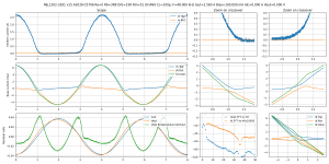
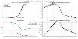
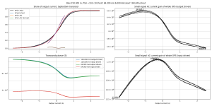
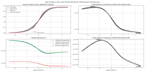
When only the NPN is ON, gm is about 3.5 S.
When only the PNP is ON, gm is about 4.2 S.
This means the NPN has about 1/3.5-1/4.2 = 47 mOhms more Zout than the PNP.
Check using the THD plot: on the second row, first column, this is the relative output voltage. It is 1.004 when the PNP is ON, and 0.997 when the NPN is ON, a variation of 0.7%..... and 0.7% of 8 ohms is 56 mOhms.
Close enough.
The NPN is on the left side of the board, the PNP is on the right, the output is on the right... Looks like we're at the point where matched trace impedances are required to get lower distortion 😀
I add a 0.05 ohm resistor in the emitter of the PNP, which flattens gm nicely. Instead of 0.7% current dependent output amplitude variation, it's down to 0.25% with a null around zero. Distortion drops a little bit.
However, emitter resistors are still evil: with just 50 milliohms, it still loses half of the class A current span on the polarity where the resistor is.
Attachments
-
 gm-Bias 100.000 m, PSU +10.0-10.0V,AC 64.000 mA 3.000 kHz,load 7.6R,HFin,LFout.png183.3 KB · Views: 102
 -
 thd-Bias 100.000 m, PSU +10.0-10.0V,AC 64.000 mA 3.000 kHz,load 7.6R,HFin,LFout.jpg771 KB · Views: 103
 -
 thd-Bias 200.000 m, PSU +10.0-10.0V,AC 64.000 mA 3.000 kHz,load 7.6R,HFin,LFout.jpg776.9 KB · Views: 109
I remove the 50 milliohm resistor, and solder a 1.5mm2 wire between the emitters.
Zout mismatch between both transistors drops from 56 mOhm to 40 mOhm.
So it looks like it will be beneficial to place the emitters on a big low impedance copper island.
I wonder if the extra Zout of the NPN comes from the fact it has the 0R15 current sense resistor in its collector, while the PNP does not... Early effect?
I tried a large capacitor (470µF) between power transistor bases. Since the circuit keeps this voltage constant, it shouldn't be a problem, unlike the "speedup capacitor".
Pros:
Slight decrease in H3 and above
Bit smoother HF current gain because both drivers drive both power transistors
Cons:
Large increase in H2 (no idea why)
Makes it impossible to vary the bias dynamically
I'm dropping the capacitor idea.
Pros:
Slight decrease in H3 and above
Bit smoother HF current gain because both drivers drive both power transistors
Cons:
Large increase in H2 (no idea why)
Makes it impossible to vary the bias dynamically
I'm dropping the capacitor idea.
Would it be worth trying a smaller cap? Maybe not a bad end result with a cap in a complete amp with feedback loop that is more effective in lower frequencies?
I'm also a bit curious of what kind of topology you are looking at for the front end of the amplifier, compensation etc? Are you planning to do similar investigations on that too?
I'm really interested what the end result will be, no doubt it will result in a good measuring amp, and most likely pleasing to the ears too. I hope I can build it sometime in the future 🙂
I tried a large capacitor (470µF) between power transistor bases. Since the circuit keeps this voltage constant, it shouldn't be a problem, unlike the "speedup capacitor".
Pros:
Slight decrease in H3 and above
Bit smoother HF current gain because both drivers drive both power transistors
Cons:
Large increase in H2 (no idea why)
Makes it impossible to vary the bias dynamically
I'm dropping the capacitor idea.
Good idea to drop it. The accelation cap, when oversized in value, is as bad as no cap, although in a different way. While a cap helps evacuating the stored charge in the bipolar base, a too large cap will slow down the turn on of the bipolars, since it trends to keep the BE junctions reverse biased, until enough charge is injected in the base from the emitter.
The cap is a trade off, between accelerating the turn off and not compromising the turn on. Usually the range of caps is quite large, but 470uF is insane. A little bit of thinking will explain why there's H2 vs. H3 at turn off/on, that's to be expected.
Thanks!
Maybe the extra distortion was due to the air-wiring, who knows, it's a mess. In the next iteration of the board I will put more space to solder extra components properly.
I want to extend the bandwidth of the output stage, and then use that bandwidth to get lots of feedback.
Bandwidth and high order feedback are a good match: if the open loop bandwidth is 30MHz instead of the usual 3MHz, that's a factor of 10, or 20dB. So, with the oldskool Cdom compensation, with open loop gain falling at 20dB/decade, extending bandwidth by 10x only gives 10x more feedback, just 20dB. It isn't a very profitable investment considering the extra circuit complexity.
But when using N pole compensation with N>1, then loop gain falls at N*20dB/decade, so that extra decade of bandwidth gives 40dB extra feedback with 2 poles, 60dB with 3 poles... And if there is a nested loop, the extra bandwidth counts for each. So if you got one outer loop with 2 pole compensation and one inner loop with 3 pole compensation, extending bandwidth by 10x gives 100dB total extra feedback instead of just 20dB, which is a huge payoff.
The first round of experimentation was about finding the output stage topology with lowest high order harmonics that feedback cannot fix. It looks like we have a winner, so the second round will be about extending open loop bandwidth. Once that is done and the bandwidth and driving requirements of whatever topology ends up winning are known, then I'll look into what kind of frontend will drive it. I have several topologies in mind, mostly standard stuff, but that's just spice simulations, so... we will see!
Sometimes I see these speed-up caps in mosfet amps. Do they make sense there?
MOSFETs do not have base current proportional to output current, so it is much simpler. You can use a large capacitor value, that will hold a constant voltage between the gates better than a smaller value. Keeping a constant voltage between the gates is a good thing, it prevents cross-conduction when coming out of clipping, by allowing the lower driver to pull on the gate of the top MOSFET to un-stick it from the rail.
However, if something happens like clipping or high frequency... that requires some gate current, then the Vbe of the driving transistors will change. If that results in the cap charging to a bit higher voltage, and the condition that resulted in that was transient and is now resolved, then the drivers have a cap between their emitters which is charged to a higher voltage than they would like, so one of them turns off and it will stay off until the cap discharges. This causes a huge increase in distortion for a little bit of time, until the cap discharges. Standard THD measurement will not catch this because the signal is static constant amplitude.
So in theory a large capacitor value would only work if you're absolutely sure that the voltage on it will be constant so it doesn't cause one driver to turn off. Also, in theory, and according to spice simulation, the 470µF cap I added to the last circuit should have a constant voltage across it, and it should make things better. But I measured a significant increase in H2.
So, hmmm...
The acceleration cap, when oversized in value, is as bad as no cap, although in a different way.
I'd say it's worse because the effects last for longer, but yeah.
The cap is a trade off, between accelerating the turn off and not compromising the turn on. Usually the range of caps is quite large, but 470uF is insane. A little bit of thinking will explain why there's H2 vs. H3 at turn off/on, that's to be expected.
With the 470µF cap, increase in H2 occurs even in the class A zone, both transistors are on, so it is not related to turn on or turn off. It also occurs when only one transistor is on, long after the other turned off. It does not happen in simulation at all.
Last edited:
Open loop bandwidth is not a relevant metric, it is the unity loop gain frequency that matters.
Increasing the compensation order is the only way to increase the available loop gain at HF, otherwise increasing the unity loop gain frequency always comes to a stability margin price, since audio amplifiers are minimum phase systems and, as a result, the loop gain and and loop gain phase are not independent variables.
I've seen some smart implementations of a 5th order compensation, but I never had the chance to measure. For DIY purposes, I would not recommend anything over the 3rd order (for example the Cherry NDFL) mostly because the higher the order, the higher the sensitivity to component values and parasitics, and the auxiliary circuitry required to tame the overload behavior, managing the conditional stability cases, etc... grows very quickly.
BTW, high order compensated amps are always conditionally stable, meaning there are always closed loop gains at which the amp is not stable. Meaning that fast transients, overloading, difficult loads, etc... may create transient of permanent oscillations. Very difficult to build something that accounts for all possible conditions. That's why you'll see very few commercial amplifiers using even a two pole compensation schema, they prefer to play safe rather than risking costly repairs under warranty. For the same reasons, unity loop gain frequencies over 1MHz in commercial amps are as rare as hen's teeth.
- Home
- Amplifiers
- Solid State
- Power amp OUTPUT STAGE measurements shootout