it's a pity it took almost half a Meg of download to see that.
haha 😱
Look at link.A Paul Kemble web page - Reider Class G.
Paul had a good write-up for it.
Thats a very well designed schematic, even D Self could learn a couple of tricks from it, have you performed any tests on it, Im particular interested in knowing if it has symmetrical clipping which it should have although its a single ended vas.
Thats a very well designed schematic, even D Self could learn a couple of tricks from it
OH Really ?
" oscillation on some models ?? - 6mhz " Cc and Cb to shunt it ! 😛 Even with slow MJ OP's. I guess I have "unlearned" these things .
OS
Thats a very well designed schematic, even D Self could learn a couple of tricks from it, have you performed any tests on it, Im particular interested in knowing if it has symmetrical clipping which it should have although its a single ended vas.
No, I have not done any tests except listening. I initially build it for subwoofer amp purpose. But eventually I got stuck to its good sonic hifi qualities.
OH Really ?
" oscillation on some models ?? - 6mhz " Cc and Cb to shunt it ! 😛 Even with slow MJ OP's. I guess I have "unlearned" these things .
OS
Cmon Os, what do we know about this amp, maybe the author built it and had problems, thats a triple outputstage, its tricky, what was his pcb layout like, we dont know these things, I bet I could get rid of those oscilations without using cc or cb and just by adding 4 resistors if required at all and changing the layout, I would use much faster outputs too. 6Mhz, that sounds just like layout problems to me, and it clearly says some models, meaning some models didnt have this problem, so what could the problem be except bad layout or grounding.
Now, what may not be apprent is that it has a chance of clipping symmetrically because of a design feature, D self still hasnt managed it on his blame has he, not even on his latest 5 th edition version of the blame.
No he hasn't , home. But he is still using the same amp for discussion. 
My philosophy on clipping is just to not let it happen (80 v rails 🙂 ) .
I do like the work , nice DIY...
OS
My philosophy on clipping is just to not let it happen (80 v rails 🙂 ) .
EXACTLY !adding 4 resistors
I do like the work , nice DIY...
OS
Last edited:
Not a very optimized design. It has redundancy everywhere. One coupling cap between each stage? electrolytic ones? These 4 stages can be condensed into justo 2 or even only one opamp stage.
Weird way of controlling volume by placing a pot in the feedback loop. It sure will bring fidelity problems, keep look as short and clean as possible.
How does it sound, by the way?
llyrroberts
if this is your A level project then I think its a damn fine effort.
Sure, you can tweak it up a bit, but the most important thing at this stage is that you are able to put a signal on the input and get a bigger, relatively undistorted signal on the output.
As for the volume control methodology, yes, its not optimum, BUT, Music Fidelity used a similar technique on one of their pre-amps and sold thousands.
Keep breadboarding and trying out stuff - its the only way to learn.
Good Luck!
Hi
This is the second build of my latest module. There is 9 seperate descrete circuits on this PCB not including the power supply. With this amp, the only thing required is a CT 34VAC transformer (the PS is on board, including the 16mA voltage doubling circuit that powers everything on the PCB except the output transistors and drivers), input signal (0.4Vp, Av~80dB) either balanced or SE (must set input selection jumper), heatsink HW, encloser, and speaker. The output is always balanced so the speaker connects across both output stages as a full bridge configuration. Since there is a pre-amp circuit included, you can use an I-pod as the signal source.😉 Ultimatly this is the intermediate proto-type as it is only 2 layers, but the next will be 3 layers, more compressed and utilize 0201 size SMD resistors instead of the 0402 size used here. About 60% of the resistors could be 0201 (1/20W) with no Pd consequences.
There are a couple of small mistakes in the PCB but I was able to repair them fairly easily. The VAS transistors consist of small signal mosfet duel pairs in SOT-563, 2N7002V & BSS84V, that work as a balanced bridge. I have outlined them with yellow in the second photo. You can't see from the picture but mounted to the sides of the small driver heatsinks are the ouput stage source resistors, TO-126 size Caddock power metal film resistors. Very nice but expensive. At over $3 each they cost much more than the output transistors
 , P-ch $1.40 and N-ch 69 cents. One neat thing about this amp is that if an output fails short and shorts the speaker output to a rail, the DC servos will steer the other speaker output to the same rail so the speaker becomes a 'bird on a wire' and is not destroyed with DC like in most circuits. It is unlikely that a fuse would blow, but they are there for good measure I suppose. The holders will fit either ATC or ATM size fuse. Given the behavior of the circuit and since the outputs are so cheap and plentiful, I did not dwell on any 'protection' circuitry.
The output stages' bias is set by the blue pot and electrically isolated by the two IL300 opto couplers (those two DIP-8 packages). The small micro 8 package duel op-amp just behind the blue pot is used to servo the opto couplers and is the only IC on the PCB. The two output stages are HEC hexfet follower stages...
This is the second build of my latest module. There is 9 seperate descrete circuits on this PCB not including the power supply. With this amp, the only thing required is a CT 34VAC transformer (the PS is on board, including the 16mA voltage doubling circuit that powers everything on the PCB except the output transistors and drivers), input signal (0.4Vp, Av~80dB) either balanced or SE (must set input selection jumper), heatsink HW, encloser, and speaker. The output is always balanced so the speaker connects across both output stages as a full bridge configuration. Since there is a pre-amp circuit included, you can use an I-pod as the signal source.😉 Ultimatly this is the intermediate proto-type as it is only 2 layers, but the next will be 3 layers, more compressed and utilize 0201 size SMD resistors instead of the 0402 size used here. About 60% of the resistors could be 0201 (1/20W) with no Pd consequences.
There are a couple of small mistakes in the PCB
but I was able to repair them fairly easily. The VAS transistors consist of small signal mosfet duel pairs in SOT-563, 2N7002V & BSS84V, that work as a balanced bridge. I have outlined them with yellow in the second photo. You can't see from the picture but mounted to the sides of the small driver heatsinks are the ouput stage source resistors, TO-126 size Caddock power metal film resistors. Very nice but expensive. At over $3 each they cost much more than the output transistors, P-ch $1.40 and N-ch 69 cents. One neat thing about this amp is that if an output fails short and shorts the speaker output to a rail, the DC servos will steer the other speaker output to the same rail so the speaker becomes a 'bird on a wire' and is not destroyed with DC like in most circuits. It is unlikely that a fuse would blow, but they are there for good measure I suppose. The holders will fit either ATC or ATM size fuse. Given the behavior of the circuit and since the outputs are so cheap and plentiful, I did not dwell on any 'protection' circuitry.The output stages' bias is set by the blue pot and electrically isolated by the two IL300 opto couplers (those two DIP-8 packages). The small micro 8 package duel op-amp just behind the blue pot is used to servo the opto couplers and is the only IC on the PCB. The two output stages are HEC hexfet follower stages...
Attachments
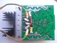
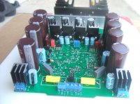
The heat sink bracket and HW is temporary. I have a much better angle bracket, 1/4" thick. Also I plan to use some small pieces of 1/2" thick white brass I have lying around for direct mount of the outputs to act as heat spreaders, then electrically insulate those from the Al bracket.
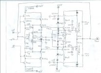
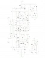
Here is the output stage circuit X 2, and the VAS. There are no Zener voltage references in the circuit, I do not like them. Too noisy. Better a J-fet bias at Idss and a resistor bypassed by a small film cap.😉
I do have to make a few minor tweaks but it seems to work nicely so far. I hope to get some real testing in before I have to leave town again, I may start a thread if anyone is interested.
Attachments
Last edited:
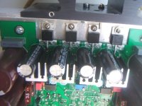
....The output transistor bias is thermally compensated by the error amp transistors so they are the only devices that need mounting, you can see in the last photo SOT-23 devices located just under the drain pin of each output. The circuit maintains a slight negative temp co, bias about ~250mA, but doesn't seem to drop below 200mA.🙂
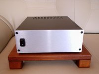
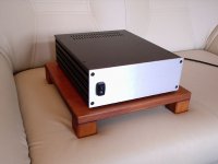
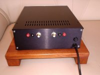
My latest...
Rod Elliott Project 3A
Some facts:
- PCB: P3A from Rod Elliott
- Output devices: MJL21193/MJL21194
- Transformer: Talema 300VA, 2x25V
- PS caps: Vishay/BC Series 056, 4x10.000uF, 63V
- Rectifier: KBPC25, 25A, 400V
- Enclosure: Galaxy 1GX288, Autocostruire, Italy
Some technical aspects:
- Quiescent current set to 75mA (50mV across resistors)
- DC offset L/R: less than 10mV each
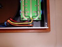
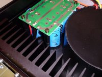
- Output devices mounted between pcb and bracket
Some pics will follow.
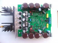
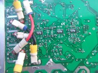
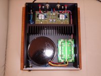
Rod Elliott Project 3A
Some facts:
- PCB: P3A from Rod Elliott
- Output devices: MJL21193/MJL21194
- Transformer: Talema 300VA, 2x25V
- PS caps: Vishay/BC Series 056, 4x10.000uF, 63V
- Rectifier: KBPC25, 25A, 400V
- Enclosure: Galaxy 1GX288, Autocostruire, Italy
Some technical aspects:
- Quiescent current set to 75mA (50mV across resistors)
- DC offset L/R: less than 10mV each
- Output devices mounted between pcb and bracket
Some pics will follow.
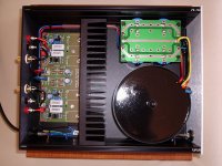

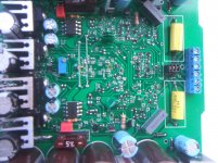
excellent work .... very neat and clean ...
---do you have scope readings of your work ?
--- is it my eyes or i see ceramic capacitors arround driver and VAS stage ???
---do you have scope readings of your work ?
--- is it my eyes or i see ceramic capacitors arround driver and VAS stage ???
- Home
- Amplifiers
- Solid State
- Post your Solid State pics here