From where this V error came ?The V5 in LTspice IV checks out.
All those tries and many versions drive-me crazy ;-) I need a little rest of one or two days.
I need to be a little more precise. Tried both the pairs 2N551/2N540 and the pairs 2SC3503C/2SA1381C. The same for the first and second stage of the diamond, that is a requisite. Same tempco result: negative. Without any tuning, the change was in the same range of result, apart the offset.
As you are certainly a lot more expert than me in simulation, I rely on you, while I will not pay you ;-)
Just the simple change of 2SC/2SA for 2N's, without the needed VBE tuning.Also check the VAS current prior to the driver in the version just posted.
Ok, lets us all synchronise on those two files .
Both open in LTS IV as well as VII.
Both the same topology and values apart the offset and quiescent tunings.
The "Pizzicato-sc one is populated with the pair: 2SA1381C /2SA1381C
Both in the input stage, VAS and driver.
No tuning of the input stage was necessary.
Here the values:
@ 27°
input: 1.22mA VAS:7.6mA, driver 10mA
HD:0.000006%
power:100mA
@ 50° ~
HD (Dlycyc= 1000): 0.000005%:
Input: 1.21mA. VAS 10mA, driver 10mA
power 74.58mA
The pizzicato-V5-2N5 was populated by the pair 2N5551C / 2N5401C
Once the offset and quiescent was tuned, (no change in the input stage) here the results:
@ 27°
input: 1.218mA VAS:7.6mA, driver 10.4mA
HD:0.000007%
power 100mA (unchanged)
@ 50° ~
HD (Dlycyc= 1000): 0.000006%:
Input: 1.216mA. VAS 10.84mA, driver 9.99mA
power: 100mA
Interesting ? No change in quiescent current on both temperatures.
Testing the BC550C as the quiescent, i got 100.4mA -> 56mA from 27 to 50°with the 2SA1381C /2SA1381C, and 100mA ->96 with the 2N5551C / 2N5401C
Testing the 546, it is not good with the 2N pairs: positive.
The original 2N3904 is the most efficient here.
Listening to your comments. Do we really need to adjust the currents of the input stage ? I have no idea to figure-it out as I have not the slightest idea of what LTS is doing with the VBE models and temp.
i'm tired of all those simulations ;-)
Attachments
Hi Tournesol,
I tried to simulate your amp, but get very strange result. Your Ltspice schematic is clattered with to many things, not easy readable. Could you show simple schematic without to much other things, I would like to simulate it, but don't want to edit it to much.
Best wishes, Damir
I tried to simulate your amp, but get very strange result. Your Ltspice schematic is clattered with to many things, not easy readable. Could you show simple schematic without to much other things, I would like to simulate it, but don't want to edit it to much.
Best wishes, Damir
Nice to see you here, Damir. Your contribution will be greatly appreciated. How is your exploration of class H ?Hi Tournesol, I tried to simulate your amp, but get very strange result. Your Ltspice schematic is clattered with to many things, not easy readable. Could you show simple schematic without to much other things, I would like to simulate it, but don't want to edit it to much. Best wishes, Damir
If you want to speed-up the sims, you could remove the Opamps, taking care to connect their Labels "Err-corr-out" & "Servo out" to the ground.
As I see, you don't like my way to arrange the schematic design ? "In fact the amp is very simple" ;-)
The box with "Voltage = Vstep" is a generator. Editing .param Vstep = set its voltage to the value you want for both the sin and square generator. The frequency is set by Freq= 1000 in the general param list. You'll need to set the dlycyc to 1000 to simulate the distortions and to be patient.
I use to pass the "op" from comments to 'spice directive' to switch from AC to trans.
You can connect or not the Middlebrook, just by moving Its labels "servo-in" and "X" and connecting-disconnecting the wire between "Inm" and "x" in the schematic. What else ?
Attachments
Last edited:
I mean .asc file not a schematic. I am just back from my holydays and I could try to show what I meant, but don't keep your breath. To many net names make difficult to read schematic.
In practical terms, the vbe of P and N devices can differ by more than 100mV. So devices would need to be selected to perform correctly. The desirable situation is for the second stage transistors to have a higher turn on voltage than the first stage. The variable resistors can then be used to achieve balance.
There is a way around this, which is to place a diode or transistor-as-diode in the emitter of the second stage and a Schottky in the emitter of the first stage. This guarantees that the second stage will be off at low current. The variable resistor can then be used to set the second stage current and vbe matching is not needed. However, there may well be some impact on performance.
There is a way around this, which is to place a diode or transistor-as-diode in the emitter of the second stage and a Schottky in the emitter of the first stage. This guarantees that the second stage will be off at low current. The variable resistor can then be used to set the second stage current and vbe matching is not needed. However, there may well be some impact on performance.
Last edited:
I will post a cleaned up asc at some point. Re-numbering will required so that the asc can be used as a build reference.
Yes, but the question I asked, spladski, with no answer is: On a statistical point of vue, what is the range of VBEs between N and P jonctions ? Like many, I believe, I never was in concern with this question and don't have a stock of active devices at the moment.In practical terms, the vbe of P and N devices can differ by more than 100mV.
Why not just just lighten the font color of 'Components text' inTo many net names make difficult to read schematic.
'Tools'-> 'Color preference' -> 'Schematic'.
That is what i do.
Last edited:
Refer to the datasheets for min, typical and max values for vbe. Apply some Gaussion distribution. I don't have figures.
Of course.Refer to the datasheets for min, typical and max values for vbe. Apply some Gaussion distribution.
Don't worry about renaming the components I was yet on it.
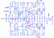
Here is the stripped down version. The focus is on the vbe issue and tempco.
You do not need to short out the Tian probe connection. When the Tian probe is disabled, it makes a pass through connection. The input should be disconnected when the probe is run, or AC amplitude and AC phase deleted from the signal generator control panel.
This version illustrates the general purpose solution that does not need vbe matching. The tempco is work in progress. Other matters are pressing so won't be back to this for a while.
Attachments
Correct. My intial solution works but relies on resistors in both the first and second stages. Resistors in the first stage do not impact gain. Resistors in the second stage impact gain and hence performance. Essentially the transistors are two diodes tied to ground sharing a current source. Inorder to balance the current, successive approximation must be used to determine resistor values making the design fussy also. The alternative is to match vbe between P and N.
The solution is to make the system more deterministic. Adding the diode to the second stage forces that stage to be off until sufficient vbe is applied by the resistor of the first stage. The Schottky has less voltage drop than a silicon diode, so the resistor makes up the difference and allows the current of the second stage to be set. Any mix of transistors can be used.
Furthermore, the solution simultaneously solves tempco. By using a transistor as diode for the second stage, its vbe drift cancels the vbe drift of the first stage. This leaves the Schottky to control tempco of the second stage. Since the solution is general purpose it should allow the cascode version to be employed. And it does.
And finally it returns to the ethos of the original proposal where the emitter resistor of the second stage can be removed completely.
I have to examine-it more deeply, but at first tries, while , if i was not making mistakes, my V6 was overcompensated, it had seem to me your version was increasing the power device current with the increase of temperature ?Furthermore, the solution simultaneously solves tempco.
(BTW: As-it, it seems the Current sources are very stable VS temp).
We still have to understand this "Time step too short" LTSPICE issue >50°.
Anyway, your idea seems very promising. I have tried on my side various ideas, with no success, distortion side. I have just now an other idea that I will try in the next days.
The idea, not examined at all, being to use the variation of voltages on the bases of the VAS BC560 & BC550 to apply some feedback to the input stage first transistors voltages, one way or an other, to compensate the VBEs variations consequences. A diamond with gain and local feedback ;-)
Thanks a lot, spladski, for all your imaginative efforts. Your collaboration is a real happiness.
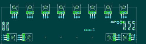
As a suggestion, when doing the layout, make a separate front end and o/p stage.
1) If you make the front end <= 100x100mm you get a very low cost pcb.
2) If you mess up one of them, the other is not affected.
3) You can make more than one type, CFA,VFA,Latfet,Vfet,bjt try different configurations at a relatively low cost.
Hafler DH-200/220 Mods
Here is the one I put together for Bob Cordell, his BC-1 design that is featured in his new book. Simple plug and play, minimize a mess of wires if I can avoid it.
Attachments
Very Excellent idea. Now please describe the electronic and mechanical interfaces to be used and I will incorporate it into the layout I have started for the output. I wish that Ostripper was around so I could get his permission to use the Class H power scheme he has worked so hard on. I am making the output interleaved PnP NpN and based on the DIYAudio heatsinks for the Big Chassis. Please lets have a vote on the interfaces soon ...ThanksAs a suggestion, when doing the layout, make a separate front end and o/p stage. 1) If you make the front end <= 100x100mm you get a very low cost pcb. 2) If you mess up one of them, the other is not affected. 3) You can make more than one type, CFA,VFA,Latfet,Vfet,bjt try different configurations at a relatively low cost. Hafler DH-200/220 Mods
Attachments
A tempco solution follows the same procedure solving vbe. I.e. making the system deterministic. Currently the tempco is controlled by the constant current source bias chain, affecting all stages. This is unlikely to yield a solution because the stage interactions are complex. We see that the first stage current source can have its own bias chain separate from the VAS cascode operating voltage. The tempco for the first stage can be made almost perfect. The tempco for the second stage is therefore the Schottky in the first stage.
Compensation elements are generally diodes and their tempco behavior can be modified by parallel resistors, reducing the slope. There is recourse to LEDs which according to color have differing temp coefficients, Red -1.5mV, Green -3.8mV, Blue -5mV.
Therefore at build time there is scope to modify the tempco behavior since simulation is a guide and cannot be trusted. The example below illustrates how the differing stages can have tempco individually targetted. The Vbe multiplier has been removed to demonstrate the overall result. This version is the cascode with second stage emitter resistors at zero, although they should be retained for the PCB, just in case.
Attachments
Yes.A tempco solution follows the same procedure solving vbe.
I was exploring a little deeper your VBE solution.
I think the esoteric matched pairs are not a requisite as long as we keep the variable resistance to set the second stage current. And we could replace the transistors you used as a diode in the second stage by a simple diode.
I attach the test file I used. Based on V6, the variation of the Adj resistance
for +0.1V in the first stage or -0.1 in the second was 274Ohms. 435 when 0V, and 441 Ohms for -0.1 in the first stage or +0.1V in the second, to keep 1.2mA current in the second stage. No real impact on distortions.
What do-you think ?
I don't know if it should be a good idea to design a separate printed board for the input stage, Ostripper like. My thought are in this amp, everything is so intimately stick together and don't it complicates the mechanical assembly ? But I will follow the opinion of the majority, just a 2 cents feeling.
Attachments
Standard T/E MTA100 or Molex KK100 style connectors and I used T/E 7.5mm lead spacing terminal blocks.Now please describe the electronic and mechanical interfaces to be used and I will incorporate it into the layout I have started for the output.
Testing all the VBE combinations on the last V6-testVBE I just poseted, each transistor of the first and second stage top between +&- 0.1V, I got The same resistances values for the same VBE differences.
190 Ohms for +0.1V in the first stage and -0.1V in the second.
274 Ohms for +0.1V & 0V or 0V &-0.1V
438 Ohms for 0 & 0
441 Ohms for 0V & -0.1V or +0.1 & 0
525 Ohms for -0.1 & + 0.1
The goal being to keep 1.2mA in the second stage.
The 1kHz HD stay the same for all combinations, 0.000007%, except for 0 & 0 where it climbs to the heights 0.00001% level. (error correction included).
Whatever the solution you will chose, between the spladski one (Without adjustments ) and mine, I consider the VBE problem has found solutions.
And about the tempco of this version, according to LTSICE, the currents in the output FETS:
-10°= 97mA
0° = 128mA
27° = 100 mA
50° = 77.5 mA
70° = 62.6 mA
75° = 59mA
How to hope better ?
Because LTSPICE consider all transistors the same temp, and that, in real life, the power devices will be hooter than the inside of the amp enclosure, I'm not sure at all that Q11 (the transistor that set the quiescent) has to be mounted on the main cooler. And pretty sure it will more comfortable on the cooler of the VAS/drivers and even no cooler at all for him.
We have to remember that the MOSFETS have a positive temp curve under somewhere between 100 & 150mA, and negative above. So they tend to auto regulate themselves.
Waiting for Spladski definitive version (If I had understood well), and the choice of all the members participating to this project between the two, this will be my definitive Version, if no issue will be found by somebody else.
Krisfr , may-be we could imagine a printed board that could allow with some straps the choice between the two ?
Pizzicato-V7.
If a moderator can be kind enough to copy-it in the first post, it should be nice. Thanks in advance.
Deep thanks to all the gentlemen who helped-me in this journey of discovery.
Next project: Offer Tintin a walk on Mars.
Attachments
I chose devices that can be either-or. My preference is for surface mount using the Diodes Inc devices. Dual transistors are not esoteric devices anymore. BCM53/56 are 34 cents from Mouser. The major vendors all have their versions.
The PCB can be laid out to accommodate duals and singles by placing the different types on either side of the PCB. I would recommend a separate PCB for the input stage. I would also recommend a numbering scheme that adds 10 to each stage. That way it is easier to track modifications and one change does not ripple through the whole schematic.
Some notes are to follow and recommendations for SMD parts. There may be a few days delay before further information can be provided.
- Home
- Amplifiers
- Solid State
- Pizzicato, a 200W low distortion CFA amplifier